stripboard · intermediate
Bias and build a two-transistor fuzz on stripboard
Trace fuzz bias, run modeled waveforms, and build a checked vero layout with three essential track cuts, exact wiring and step-by-step screenshots.
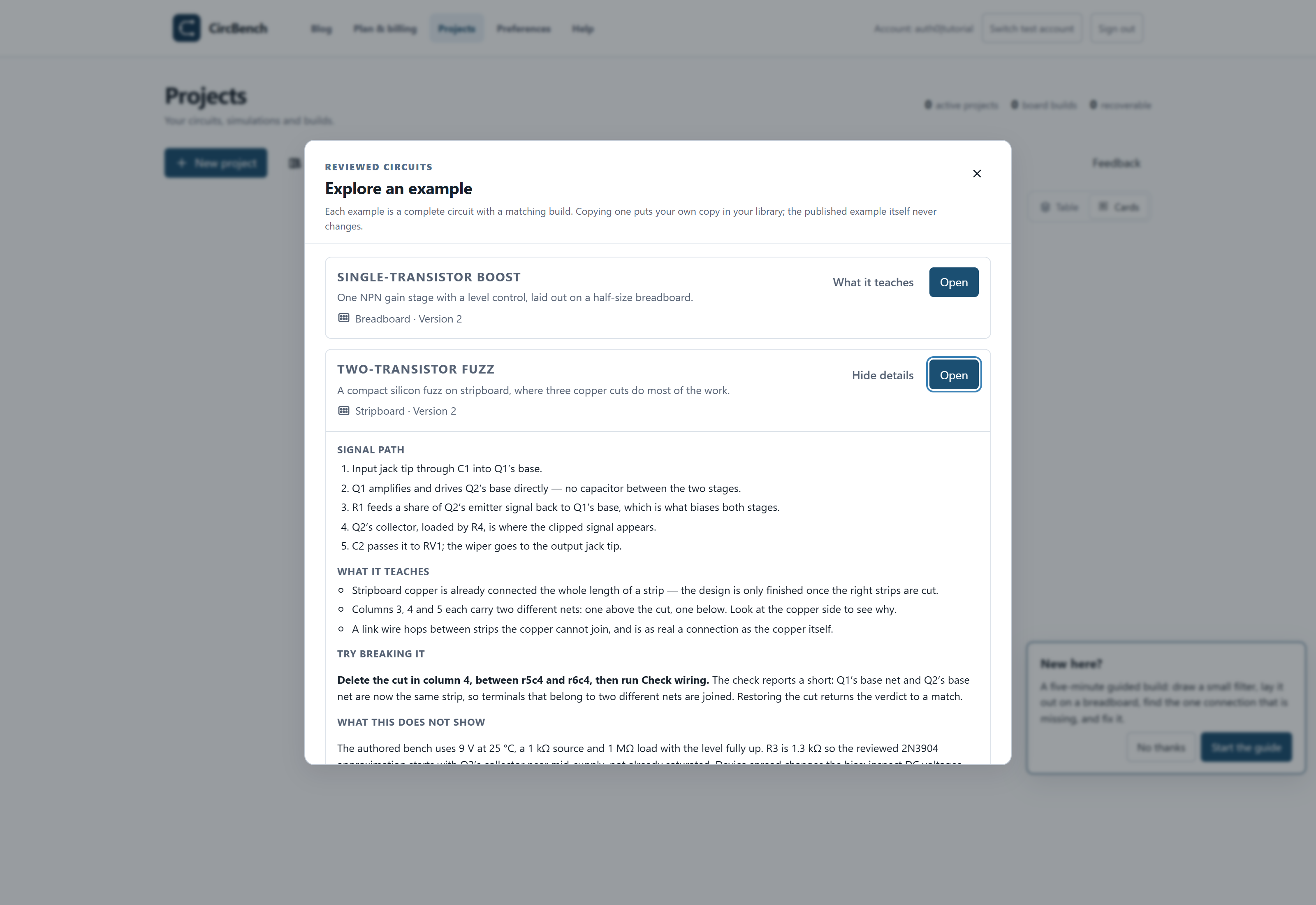
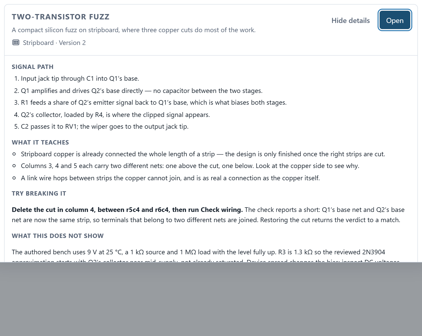
The app opens the current example chooser. Choose Open to create your own account copy. For this guide's exact v2, download and import the project backup if the catalog version has changed.
Stripboard copper is already connected before you place a part. This makes track cuts as important as jumpers. You will follow a directly coupled two-transistor fuzz, inspect its DC bias and driven waveform, then reproduce a 12 × 10 vertical-strip layout. The deliberate missing-cut experiment shows why an orderly board can still contain a short.
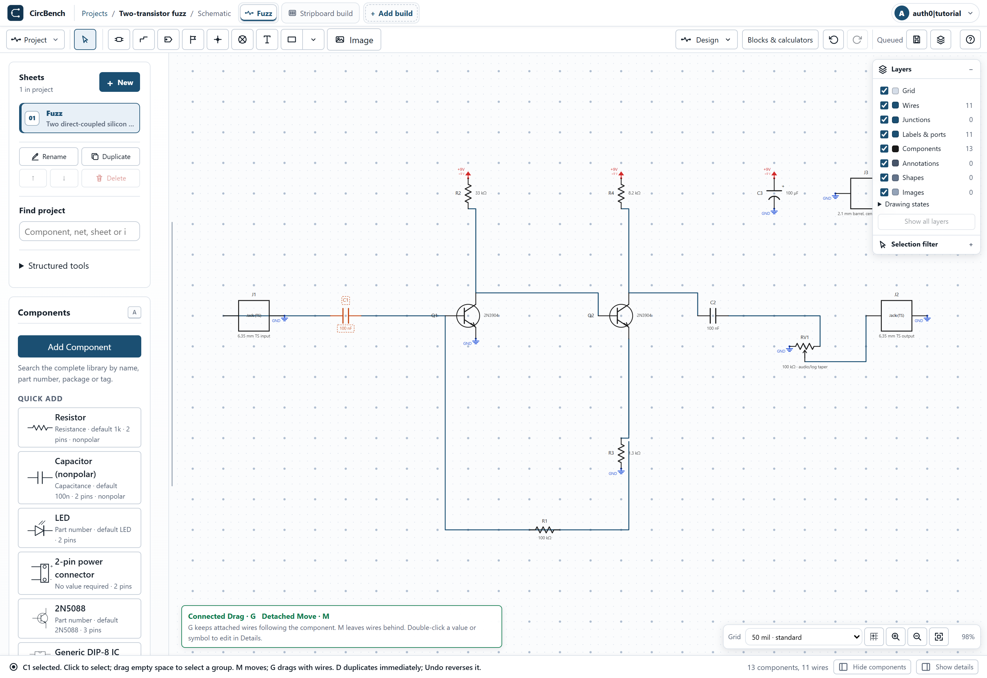
Parts: Two 2N3904s; R1 100 kΩ, R2 33 kΩ, R3 1.3 kΩ, R4 8.2 kΩ; C1/C2 100 nF, C3 100 µF supply filter; A100K level control and panel audio/DC hardware. This guide requires v2; the older v1 used 470 Ω for R3.
Before starting: have a CircBench account and use a copy for experiments. This is a software build and simulation walkthrough; the images are actual application screenshots, not photographs of assembled hardware. Every numbered step has a detail image and a link to its unmodified full context PNG. Open full size when comparing small pin labels, especially on a phone.
Draw and understand the schematic
1. Open the exact reviewed example
Use the example link above, sign in if requested, and confirm Two-transistor fuzz, version 2 in Explore an example. Choose Open to create your own account copy. The link alone does not create a project. If the catalog changes, import the versioned backup above to follow this precise guide. All screenshots show the actual reviewed copy, with completed wiring as a reference for your own drawing.
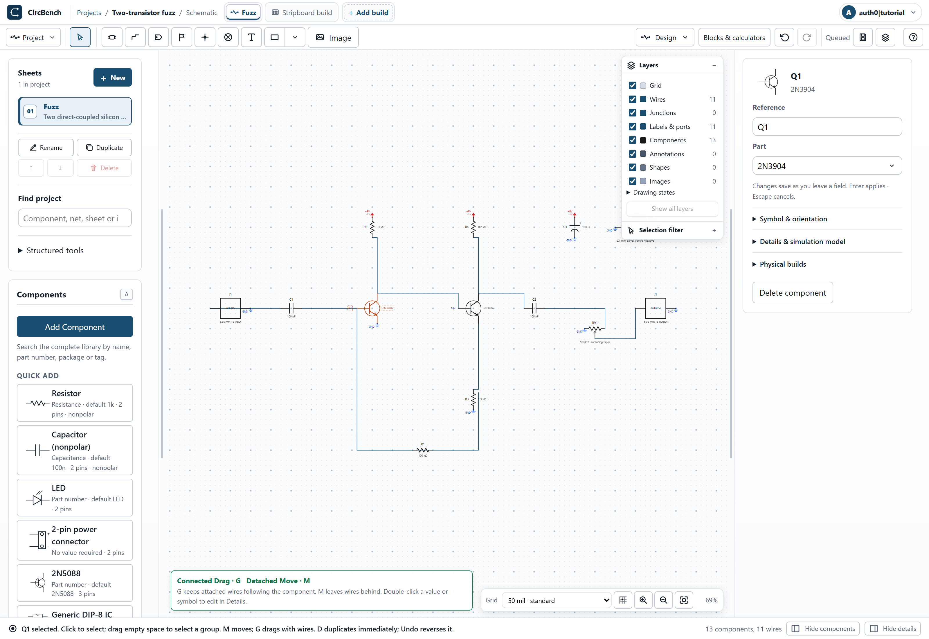
2. Identify both transistor stages
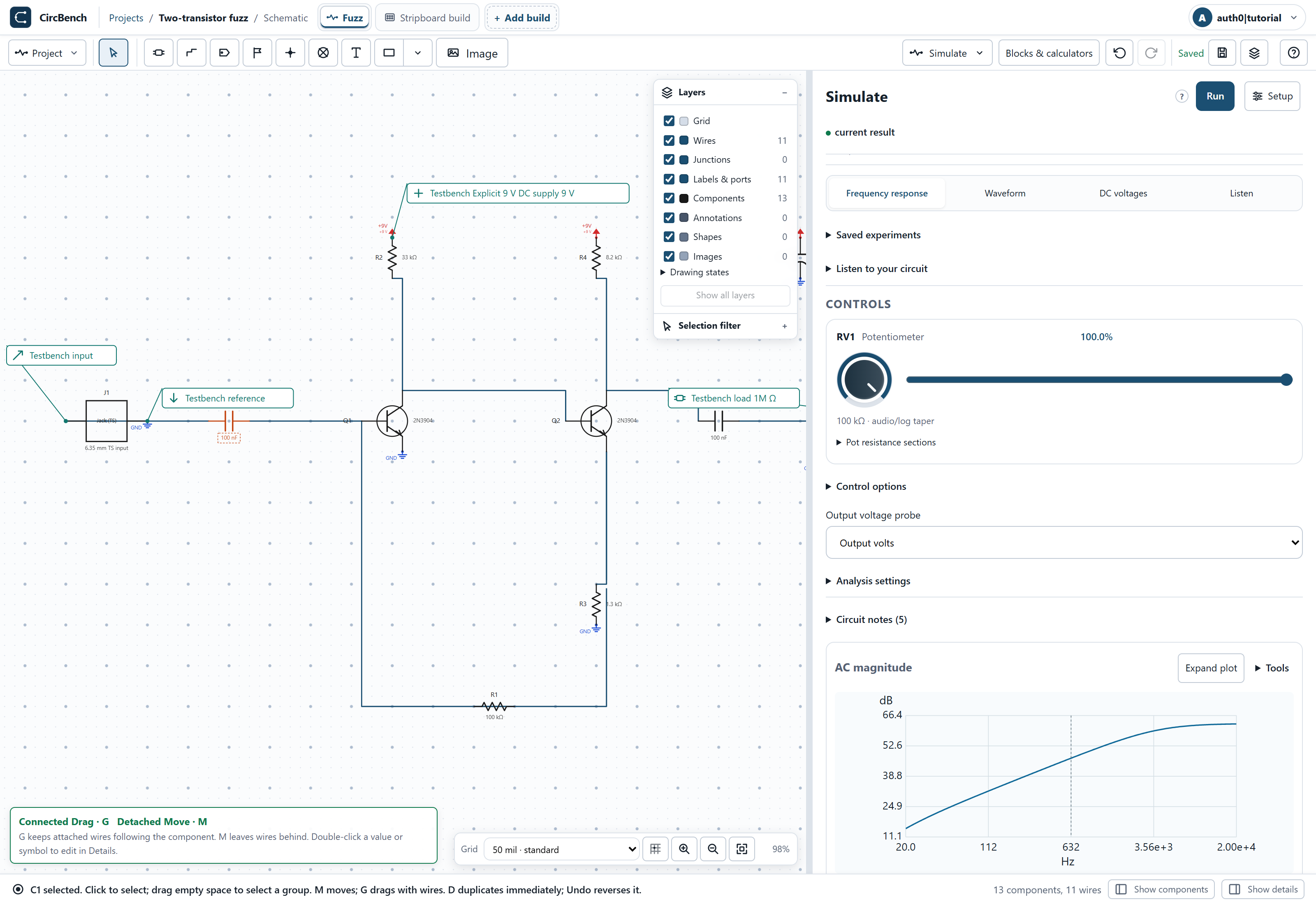
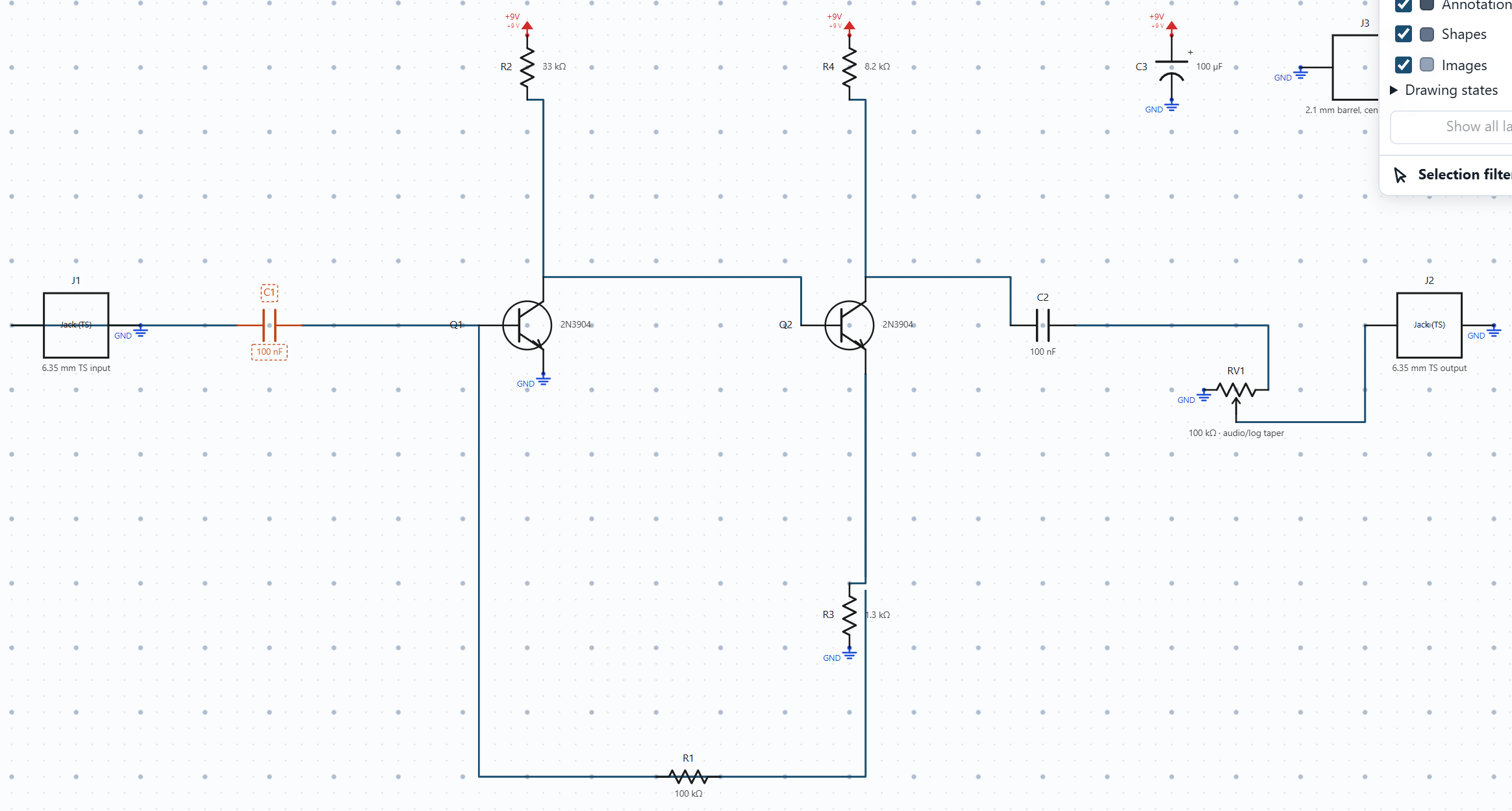
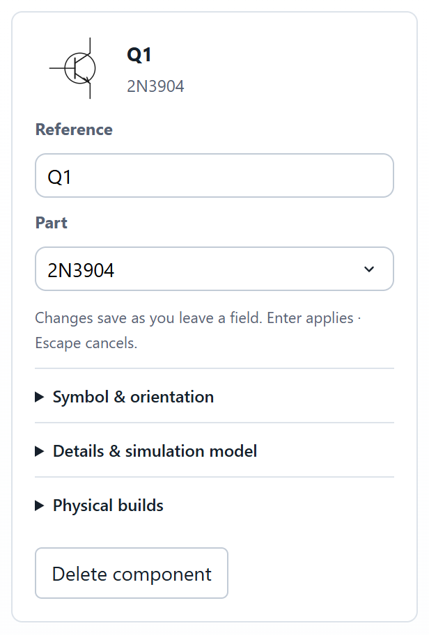
Inspect Q1’s E/B/C identities, then compare Q2 on the schematic. A redraw begins with two 2N3904s whose emitter nets remain distinct. Q1 collector connects directly to Q2 base. Do not insert an extra coupling capacitor there: the direct connection establishes the second stage’s DC conditions as well as its signal path.
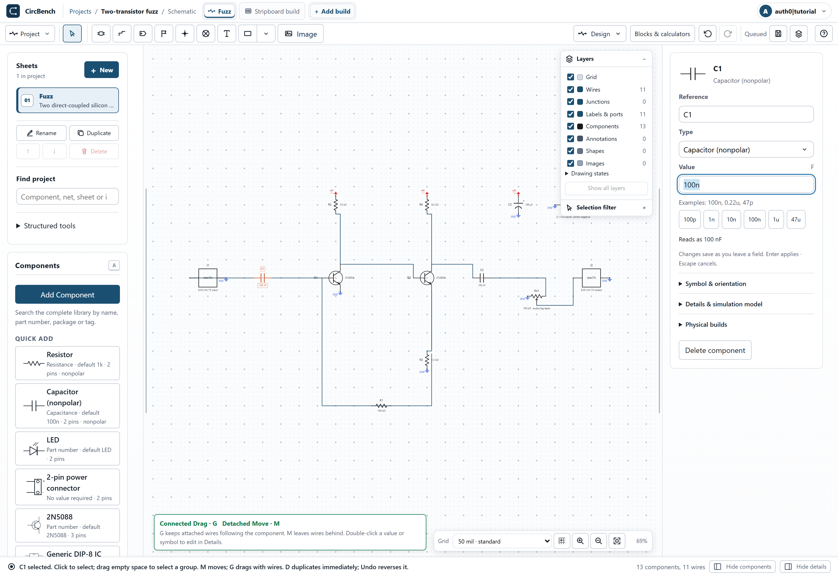
3. Build coupling, feedback and bias
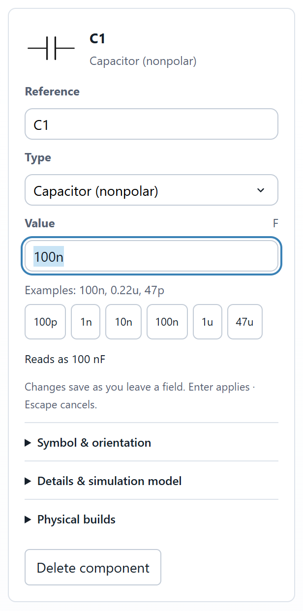
Inspect C1 and confirm 100 nF from input to Q1 base. Connect R1, 100 kΩ, from Q2 emitter back to Q1 base. Use R2 33 kΩ, R3 1.3 kΩ and R4 8.2 kΩ exactly as the full drawing shows. Confirm R3 explicitly; a v1 copy with 470 Ω gives a different bias.
4. Complete the full fuzz drawing
Fit the schematic. Follow the direct Q1-collector/Q2-base connection, then the feedback from Q2 emitter to Q1 base. Couple the output through C2, 100 nF, to the level control, with wiper to output and track bottom to return. Add the 100 µF supply filter with positive to 9 V. Join panel returns explicitly.
Configure and interpret the simulation
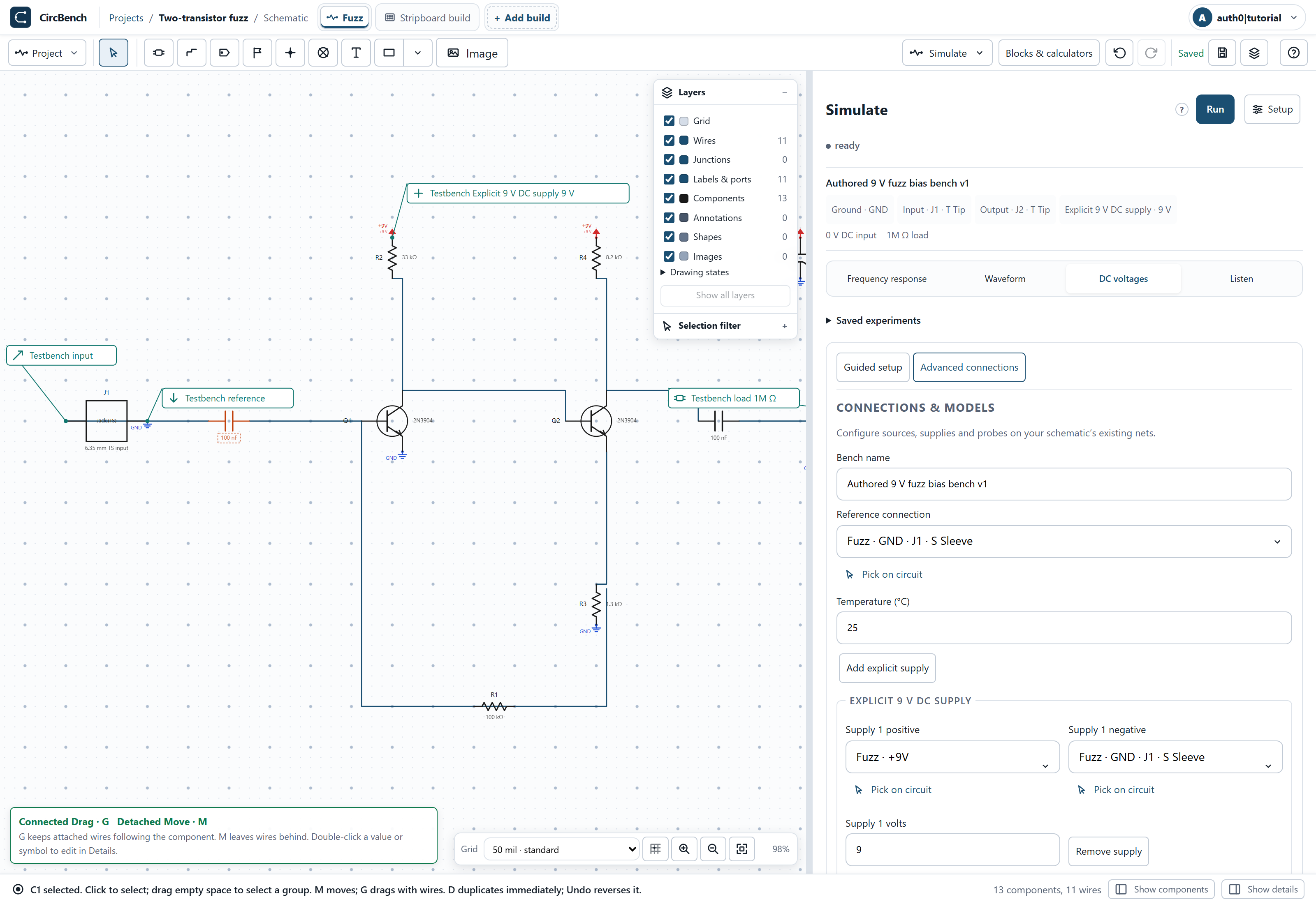
5. Set the authored fuzz bench
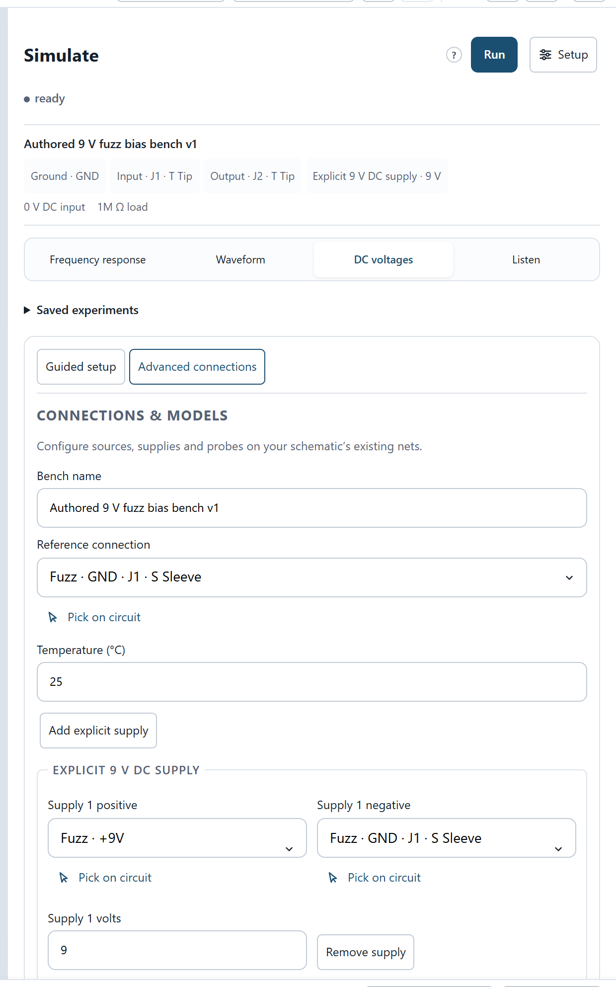
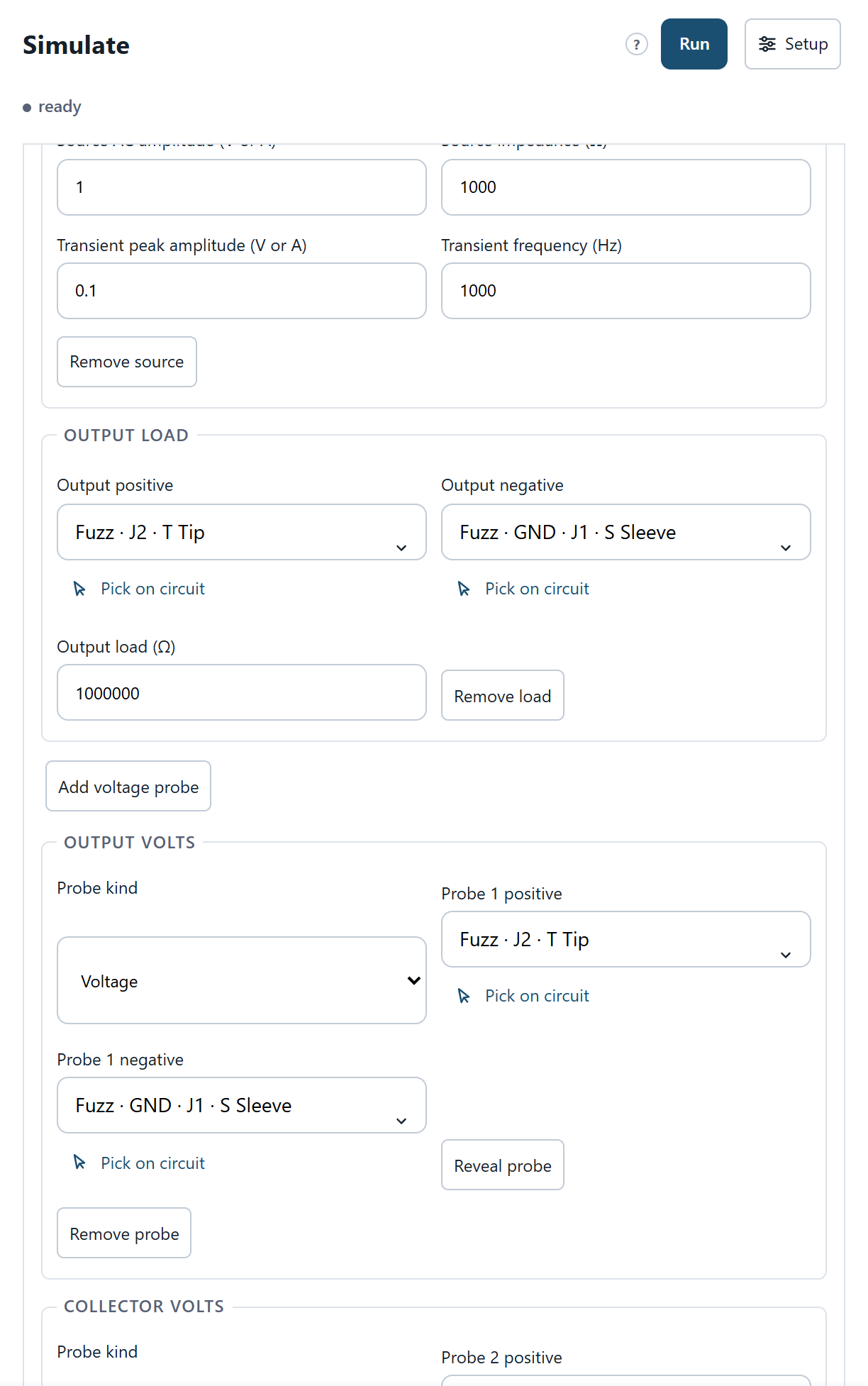
Choose Simulate → Setup. Retain explicit 9 V, 1 kΩ source, 1 MΩ output load, full level, 25 °C and a 100 mV-peak 1 kHz sine. Verify reference/input/output and supply endpoints. Select the reviewed 2N3904 approximations deliberately, then save. Missing models or a missing reference must be resolved before an analysis can be interpreted.
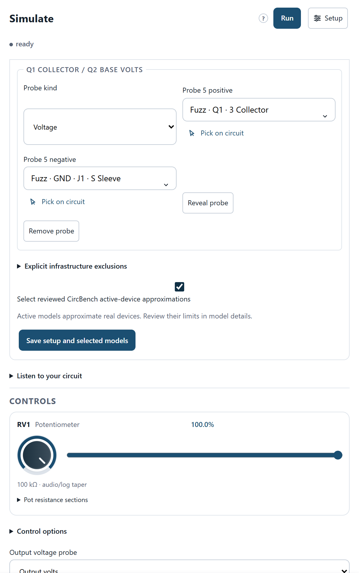
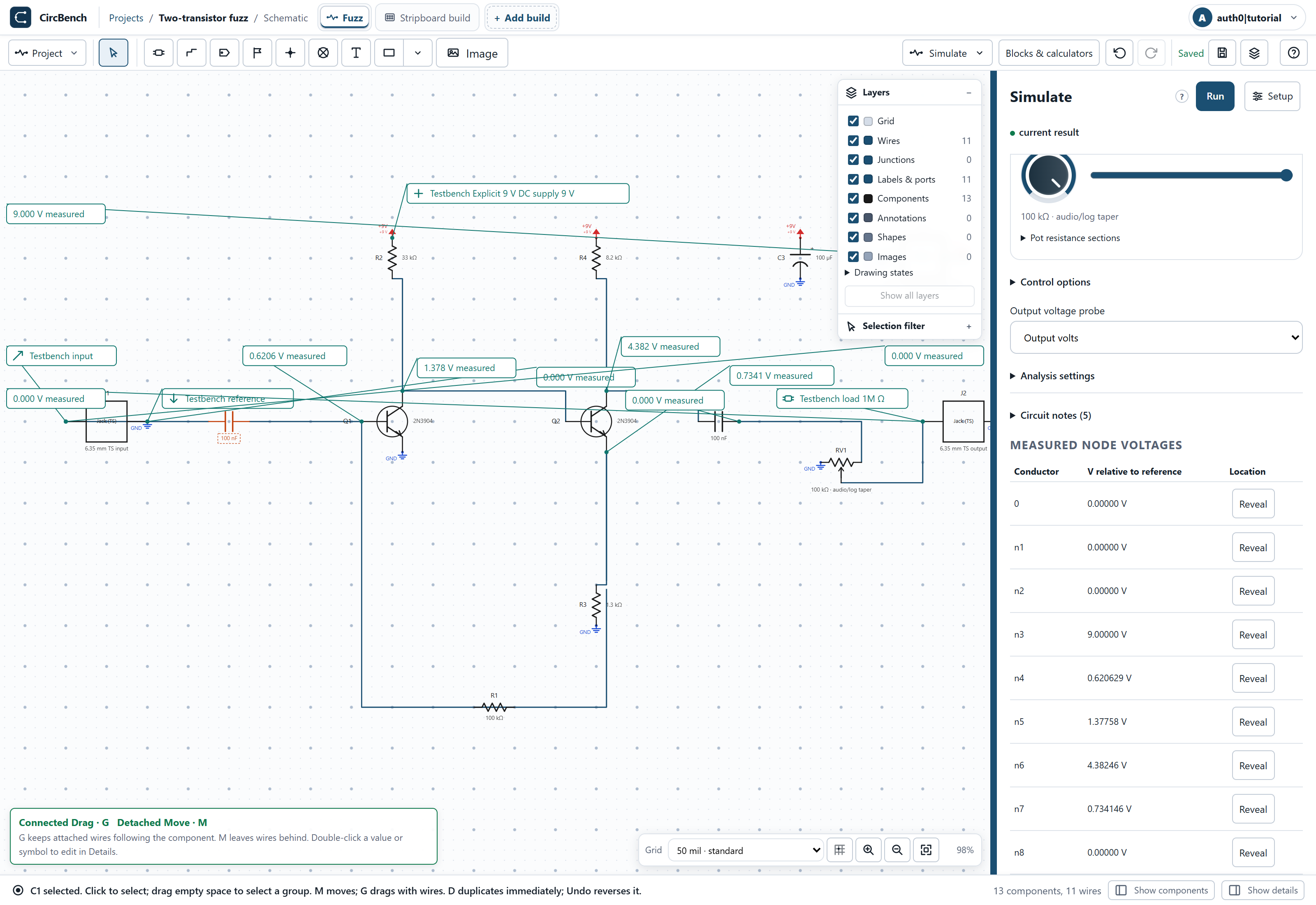
6. Check the second collector bias
Run DC operating point and wait for current result. Reveal the Q2 collector node: the captured nominal setup gives about 4.38 V, within the reviewed 4–5 V range. Inspect the Q1 collector/Q2 base and both emitter nodes too. These are coupled bias conditions; changing R3 or treating the emitters as one net changes the circuit.
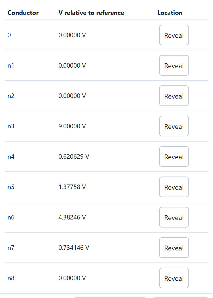
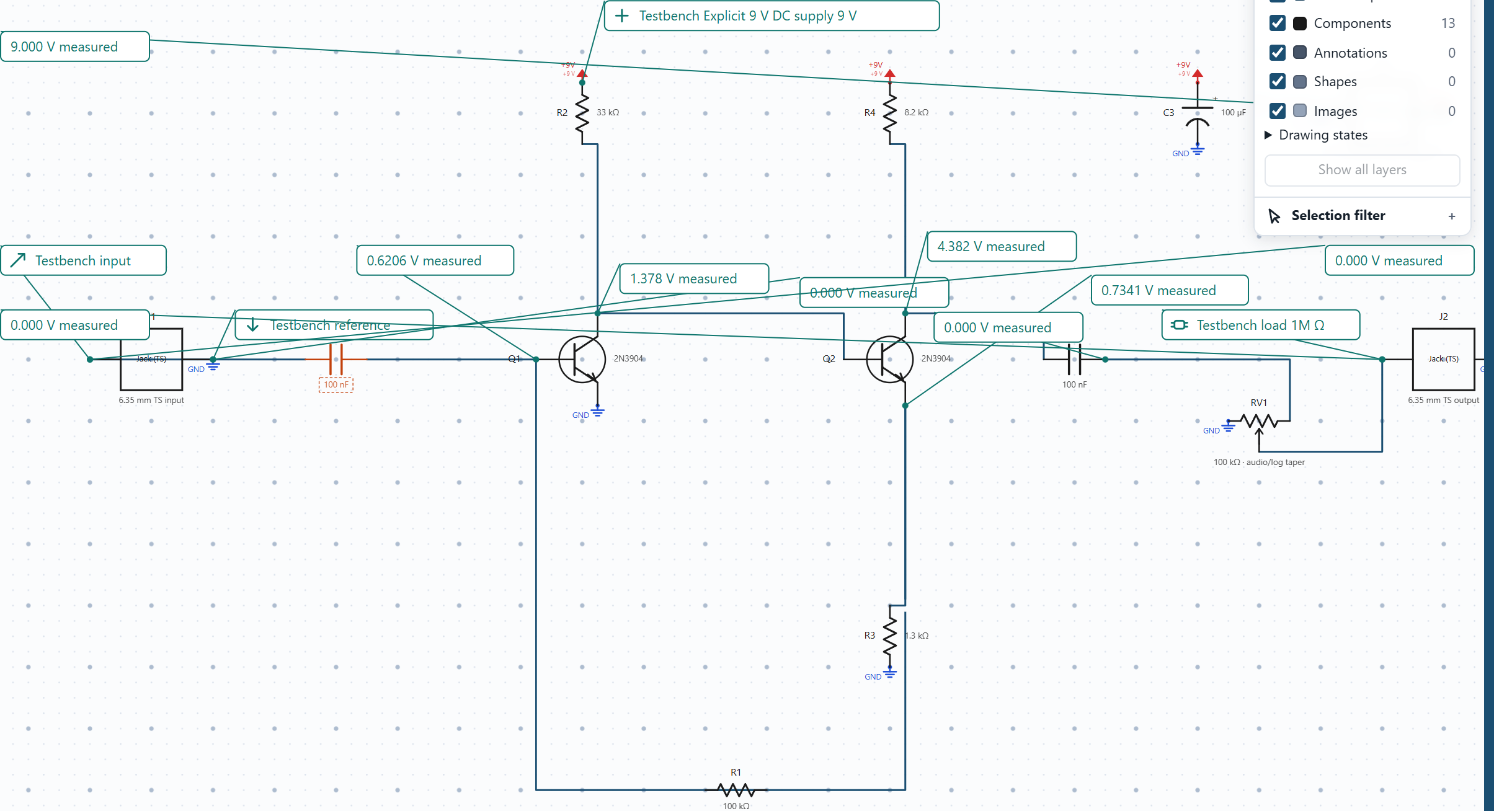
7. Separate small-signal response from fuzz
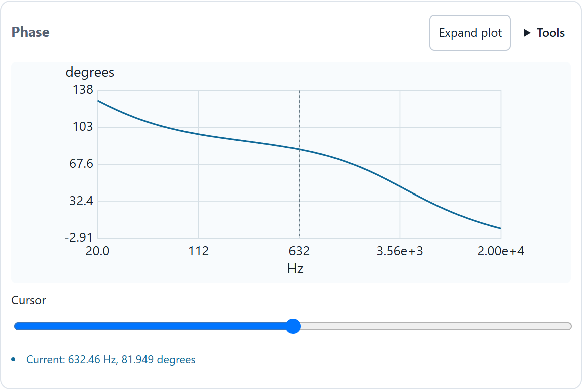
Run AC frequency response over 20 Hz–20 kHz. Inspect gain and phase separately. AC is linearized around the current operating point; a large small-signal gain does not imply an equally large clean output for the 100 mV input. The next step uses nonlinear transient behavior to expose the available swing.
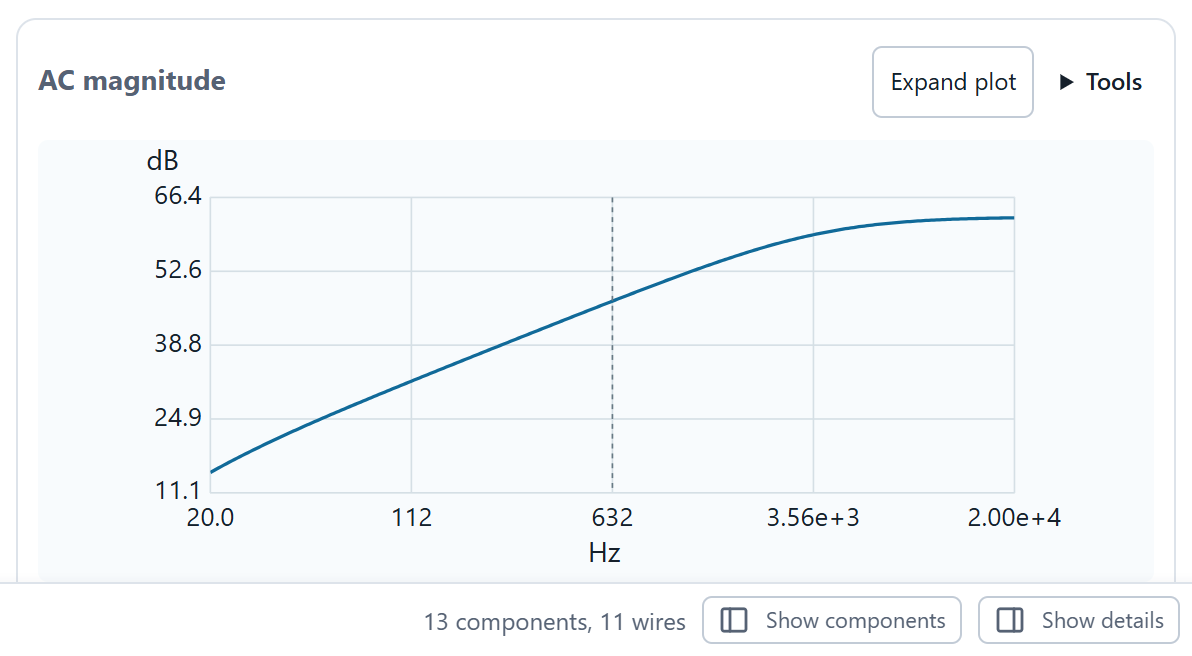
8. Inspect the driven waveform
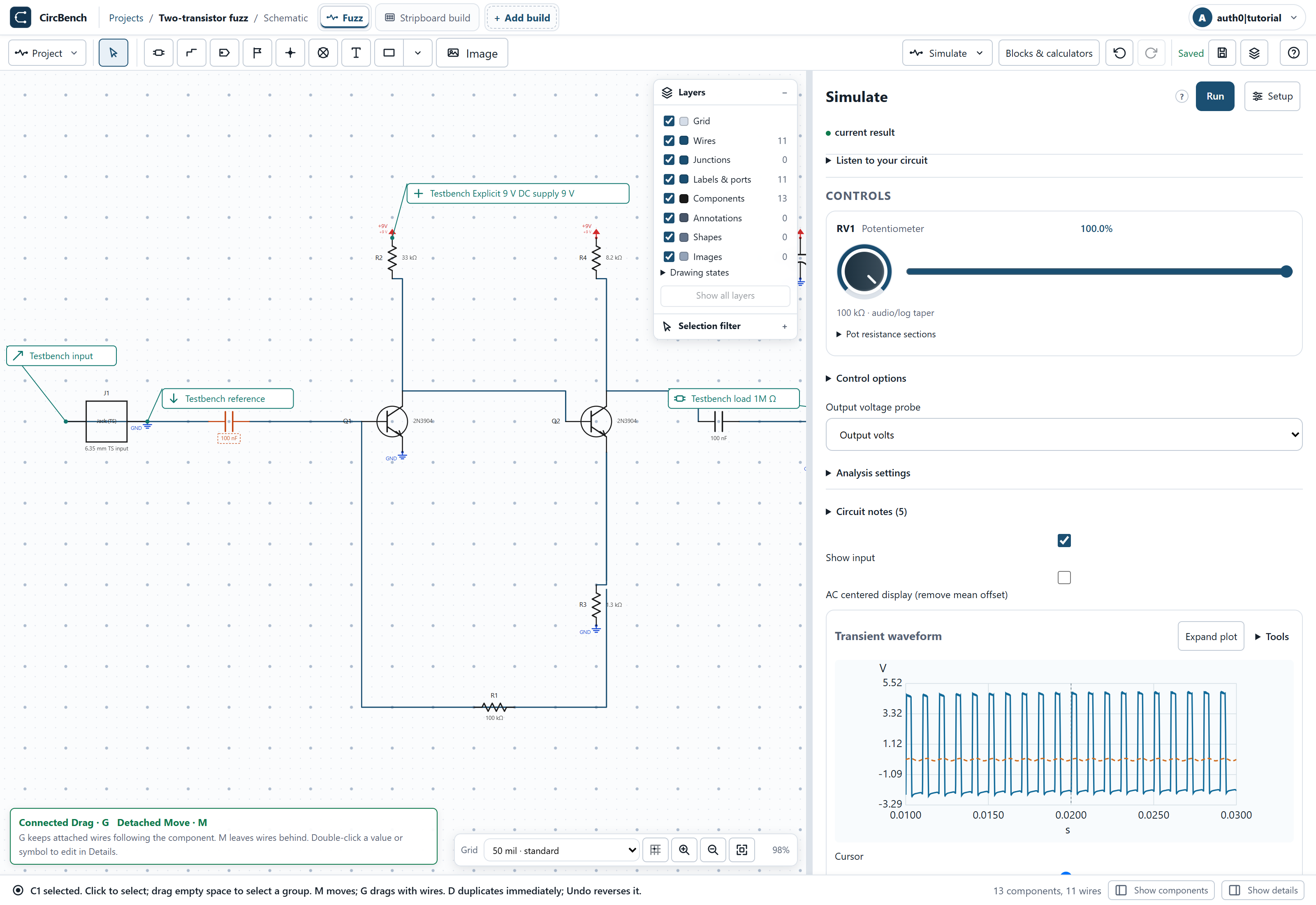
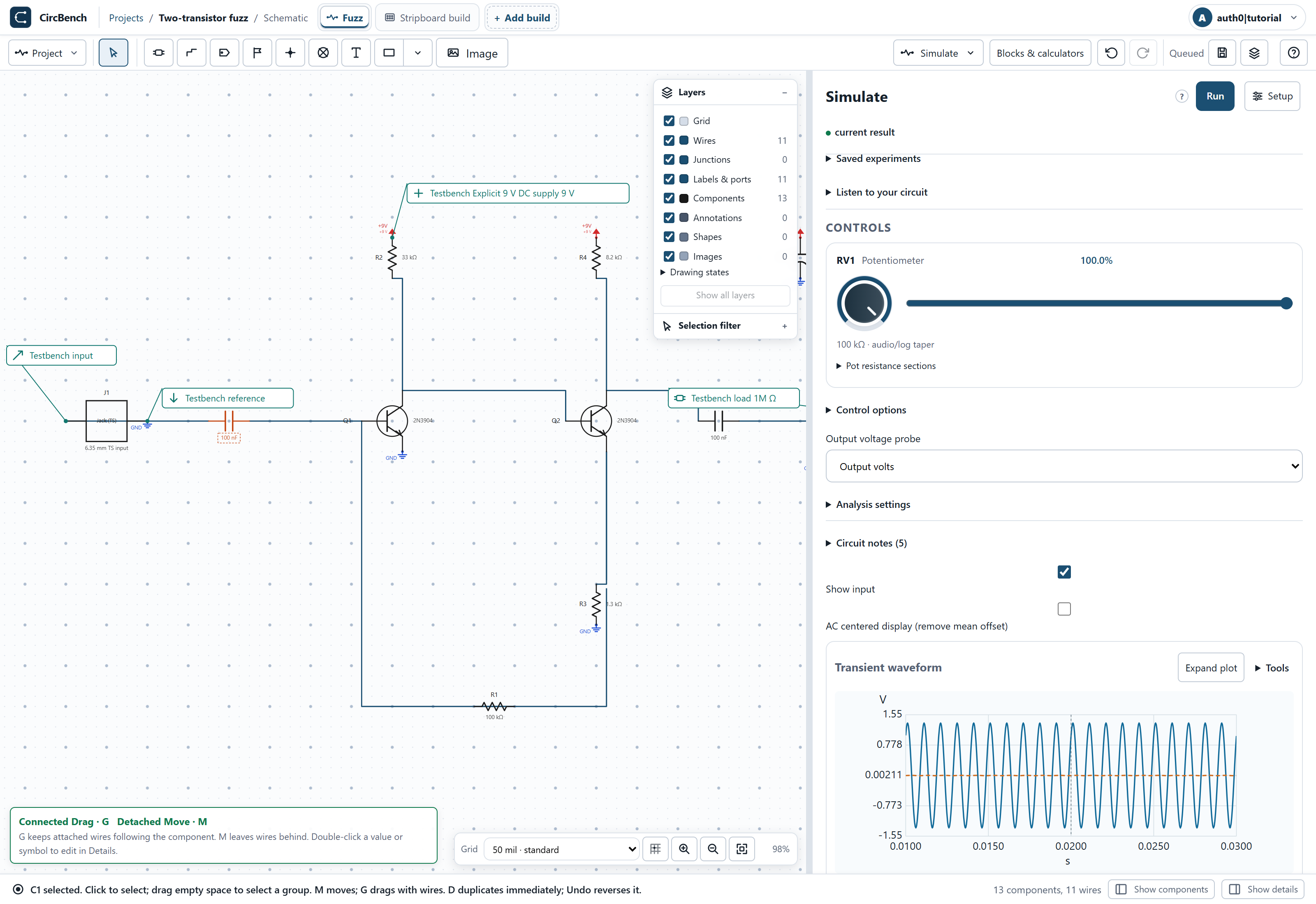
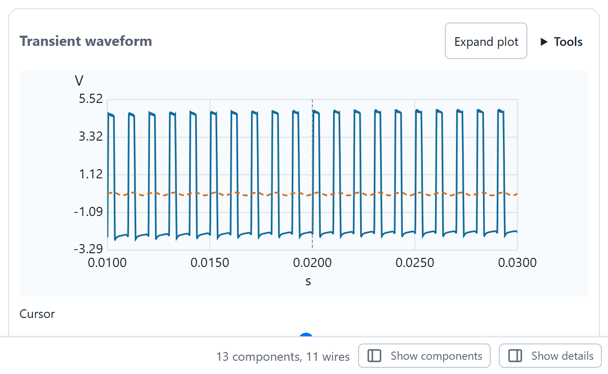
Run Transient waveform with the authored 100 mV-peak 1 kHz input. Compare the small dashed input with the much larger, asymmetric output. The shape is a result of the nominal modeled circuit and bias. Do not label it a hardware recording or infer a particular pedal sound from a normalized plot.
9. Compare a smaller drive
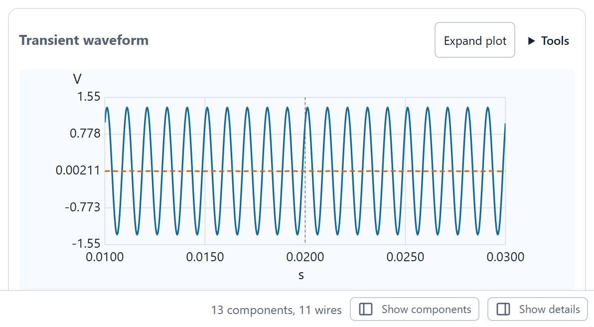
Change Transient peak amplitude to 0.005 V in Setup, save and run a fresh waveform. Compare its shape with the 0.1 V case while keeping supply, level and load unchanged. Restore 0.1 V and save afterward. Restoring settings makes the last comparison previous; rerun if you need a current response for the restored bench.
Build the physical layout
10. Choose vertical stripboard and its face
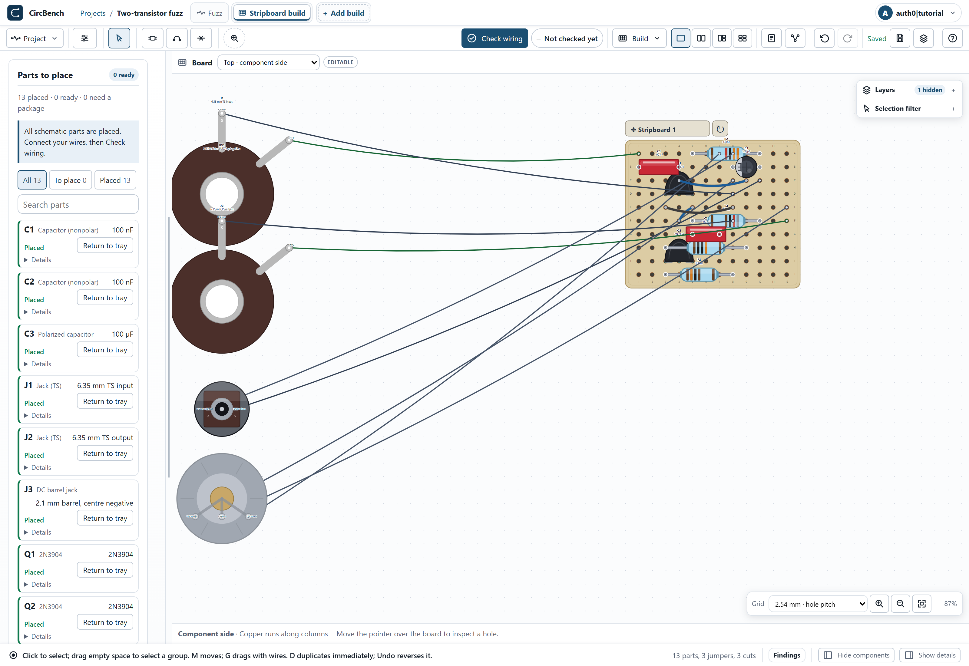
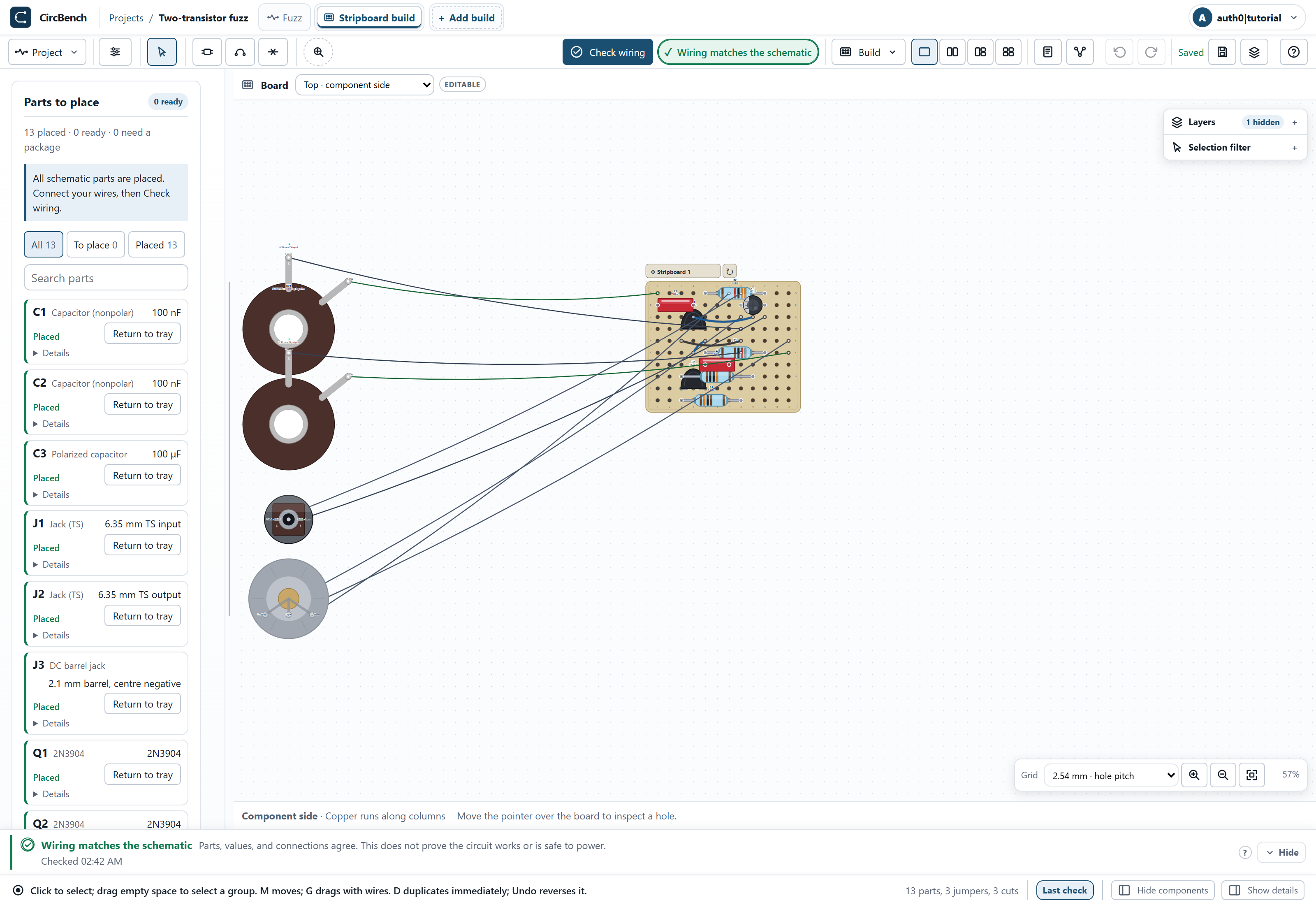
Open Stripboard build and Fit board to window. The reviewed template is 12 columns × 10 rows with vertical copper. On the component face, rows A–J map to internal rows 1–10. A column initially shares copper; neighboring columns do not. Keep this orientation while reproducing the placement.
11. Place transistors on their mapped contacts
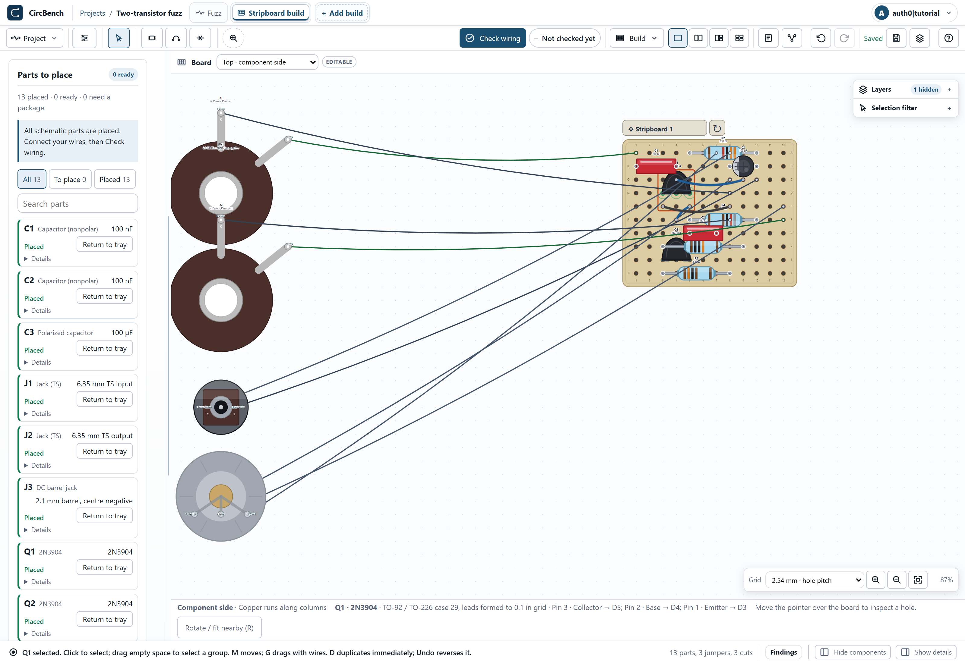
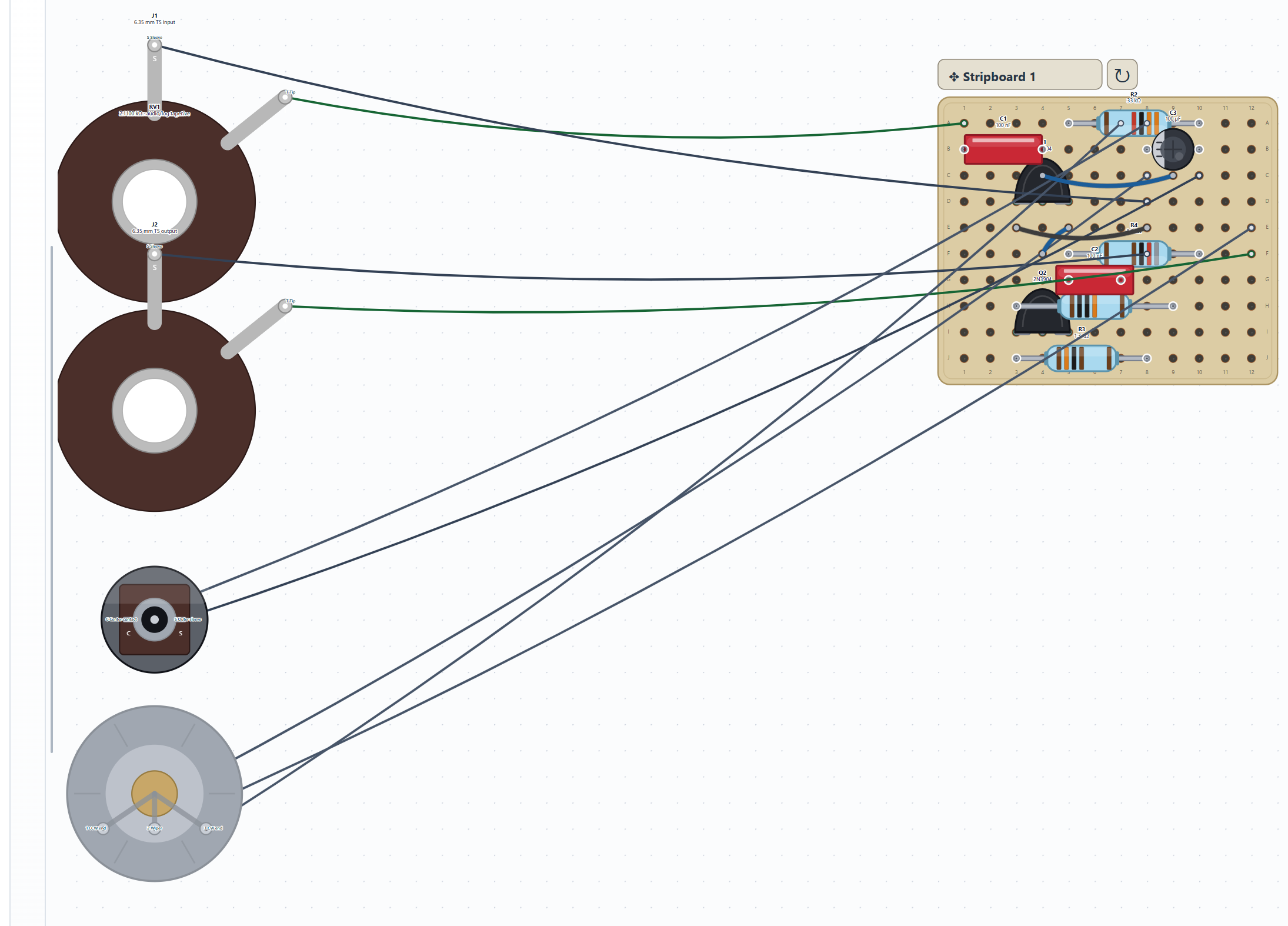
Q1 E/B/C go to D3/D4/D5; Q2 E/B/C go to I3/I4/I5. Confirm logical pins, fitted package terminals and board contacts separately. Use the exact resistor/capacitor attachments in the schedule below. Position alone does not prove a terminal mapping, especially if you substitute another physical transistor package.
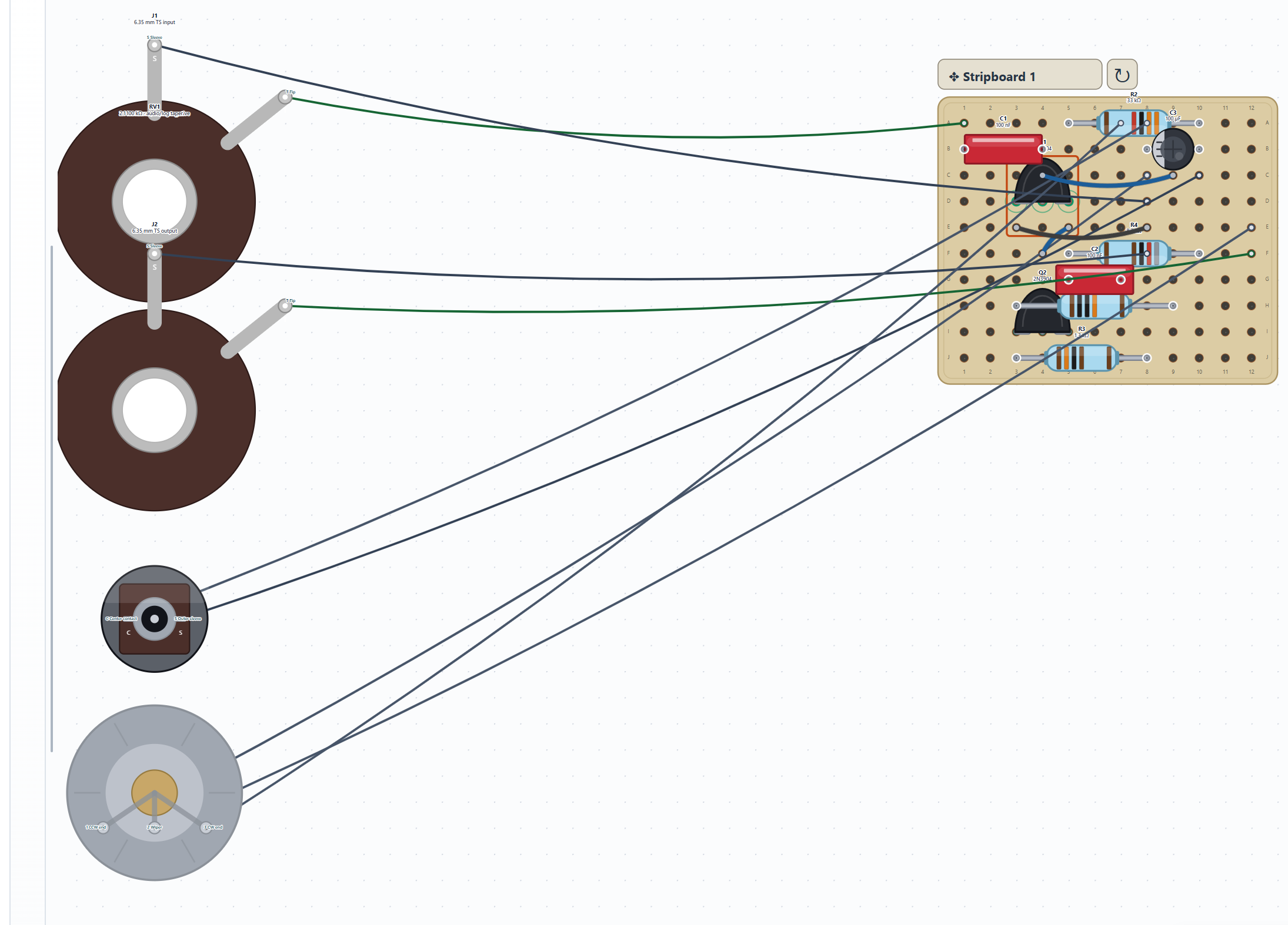
12. Make all three essential track cuts
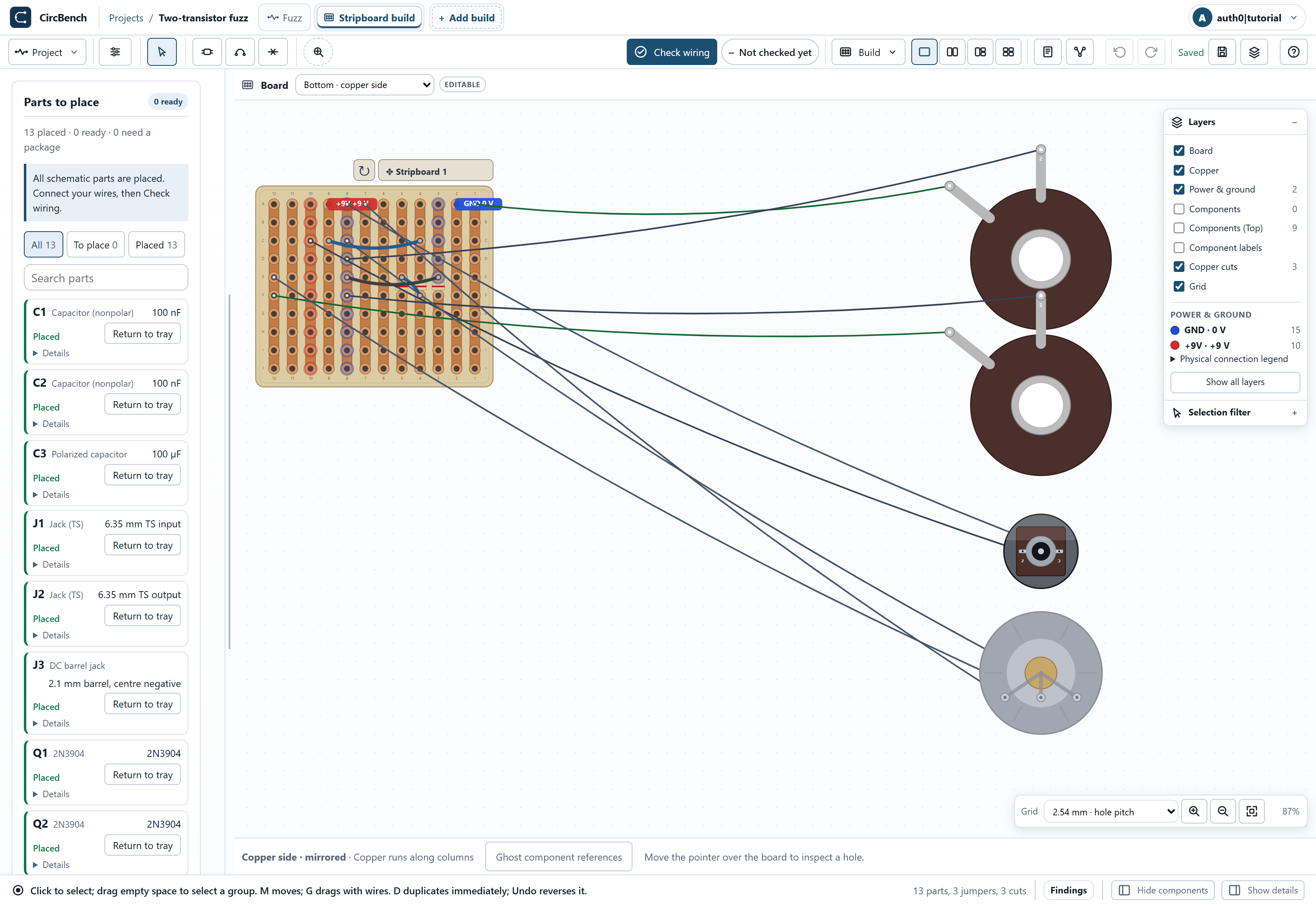
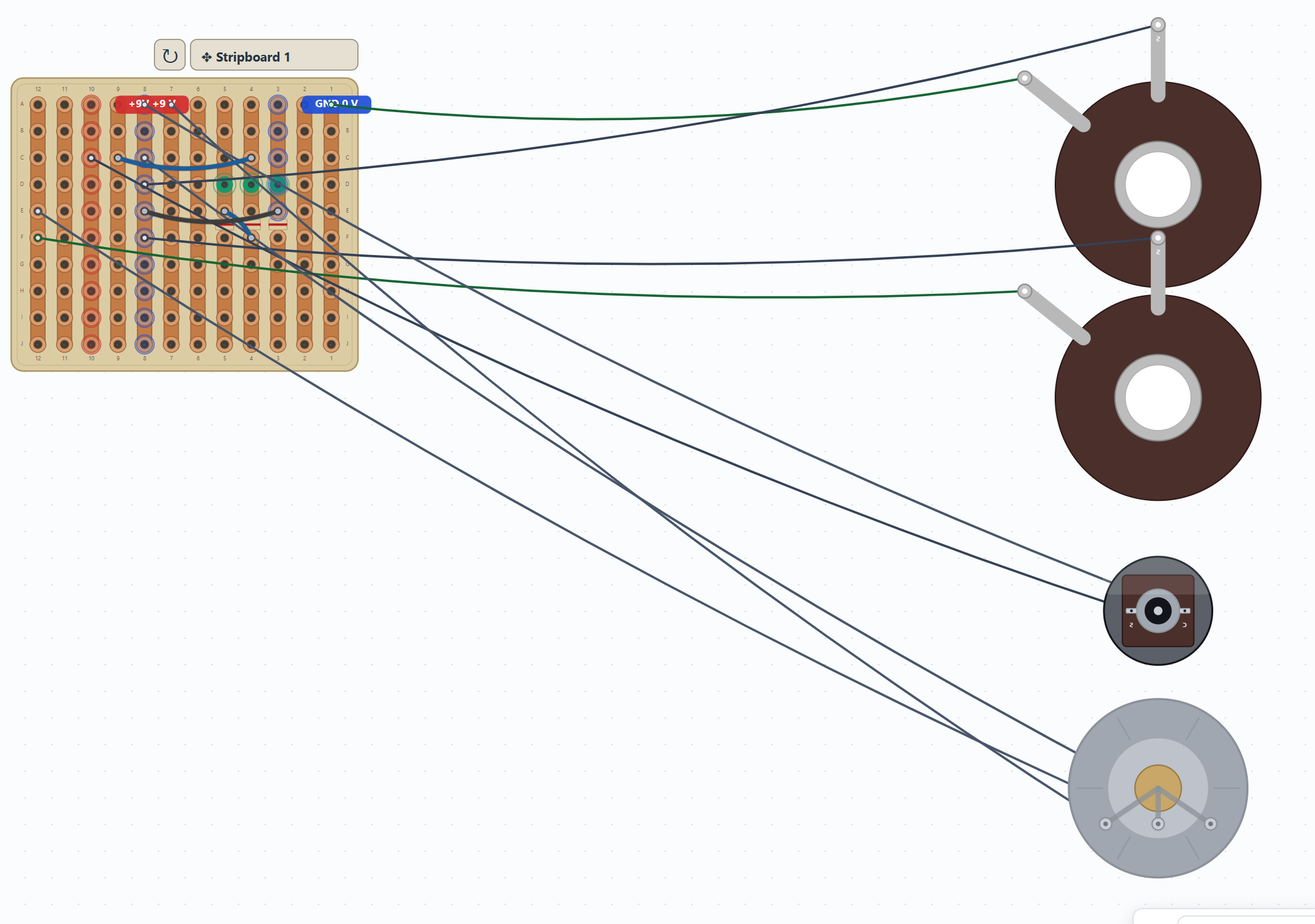
Select the copper face and inspect the enlarged contacts. Cut between E3–F3, E4–F4 and E5–F5: internally rows 5/6, columns 3/4/5. These are between-hole cuts, not removed holes. The face is mirrored horizontally, so follow its labels. Without the column-4 cut, the two base regions remain one continuous conductor.
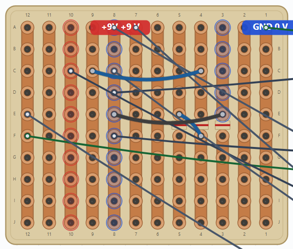
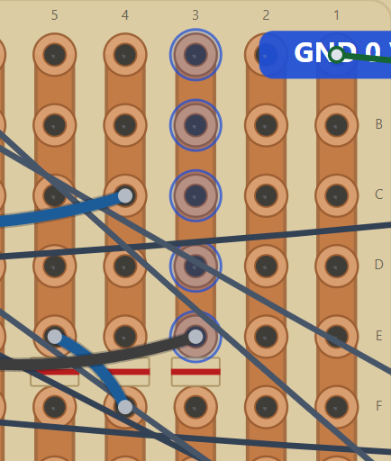
13. Add links and the panel harness
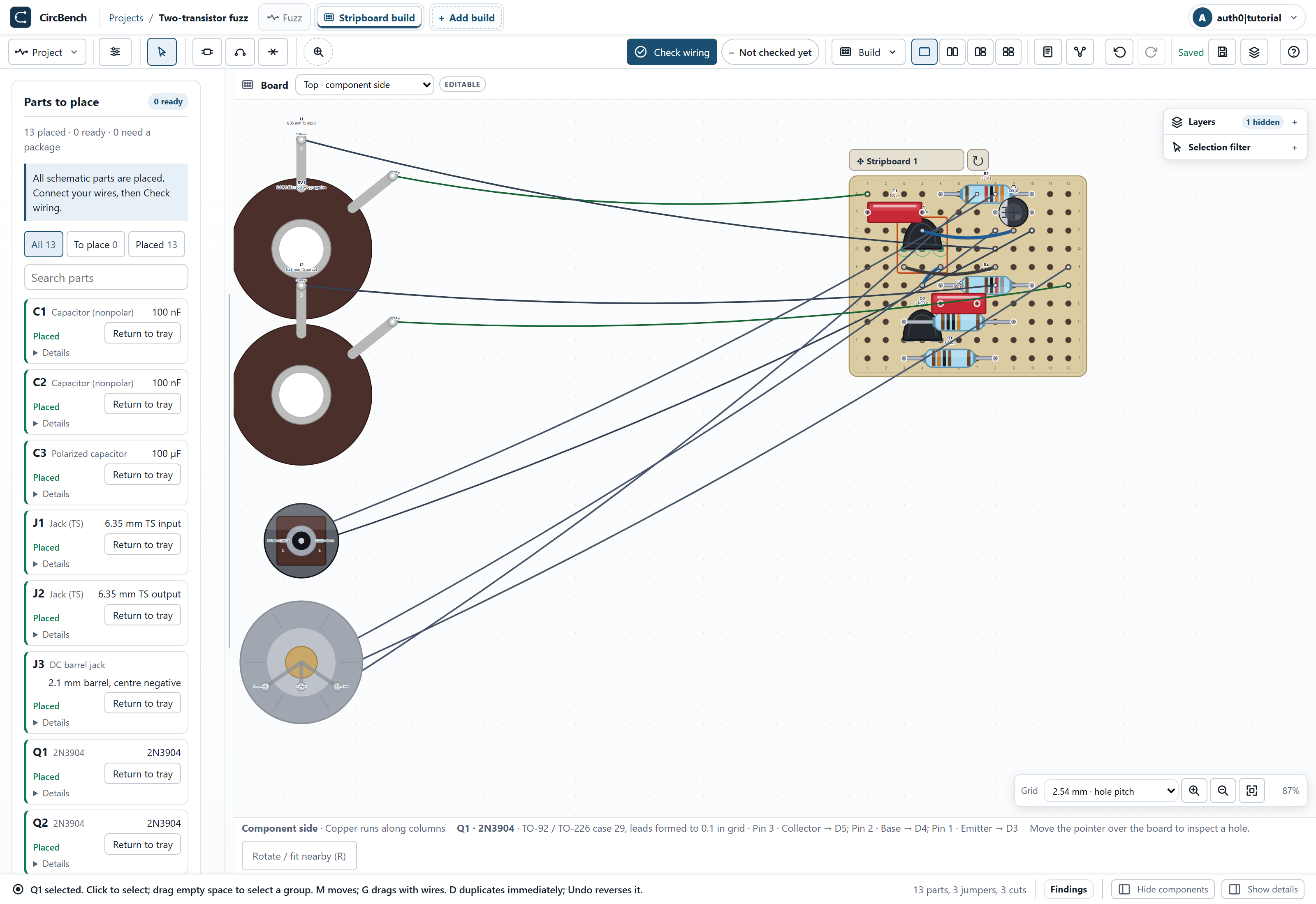
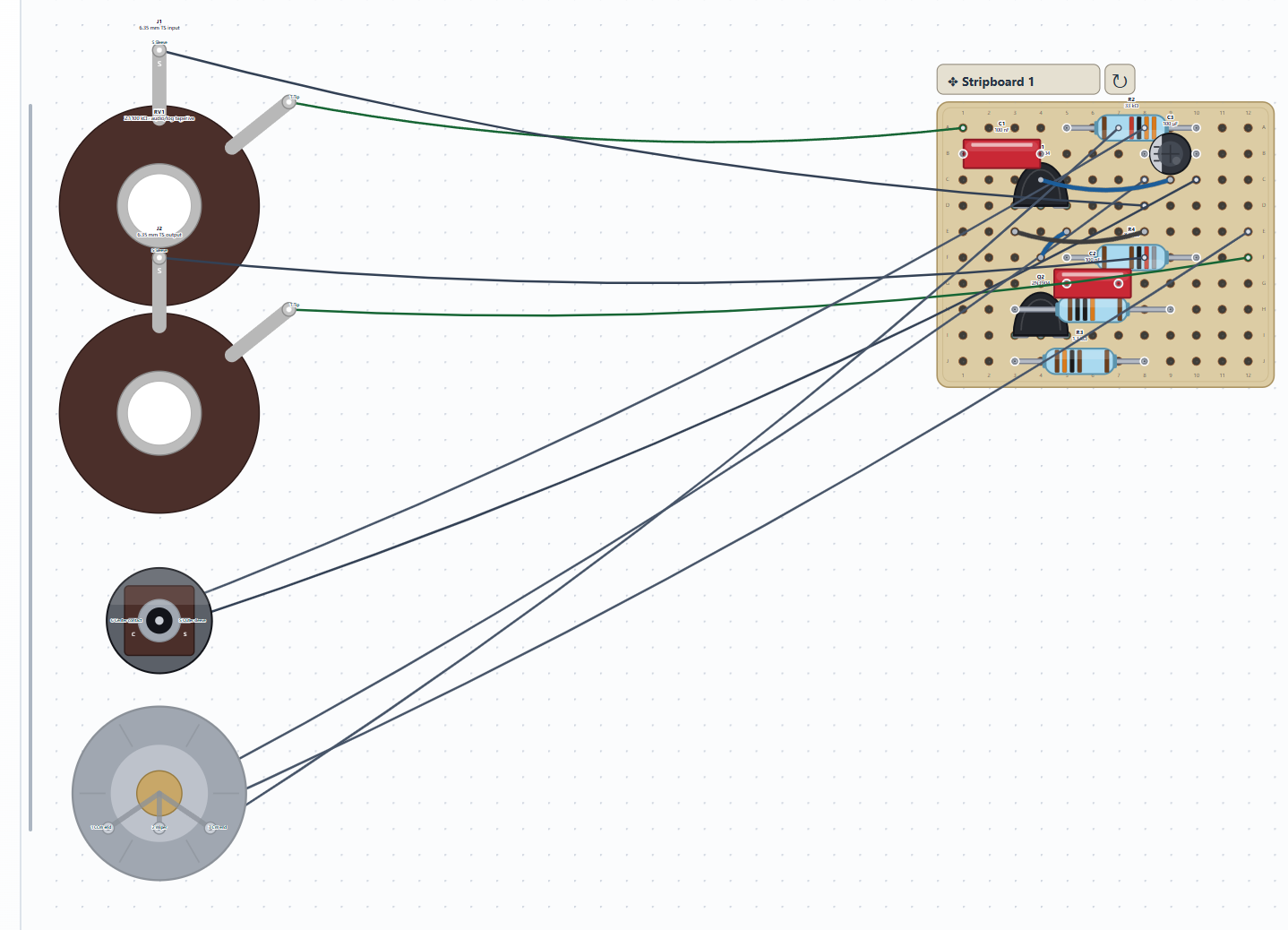
Return to component view. Add E5–F4, C4–C9 and E3–E8 as insulated links; they bridge specific nets across the divided strips. Reproduce the jack, pot and power attachments in the schedule below. Trace 9 V, return, input, feedback and output against the schematic before a new wiring check. Verify the electrolytic’s polarity.
Exact reviewed connection schedule
The following tables come from the same versioned backup. Terminal identities belong to the fitted part; letter/number contacts belong to the board. In the copper view the picture mirrors, but these labels retain their identity.
| Part | Logical terminal → board contact |
|---|---|
| Q1 | E → D3; B → D4; C → D5 |
| Q2 | E → I3; B → I4; C → I5 |
| C1 | 1 → B1; 2 → B4 |
| R2 | 1 → A10; 2 → A5 |
| R4 | 1 → F10; 2 → F5 |
| R3 | 1 → J3; 2 → J8 |
| R1 | 1 → H3; 2 → H9 |
| C2 | 1 → G5; 2 → G7 |
| C3 | + → B10; - → B8 |
| J1 | T → A1; S → D8 |
| J2 | T → F12; S → F8 |
| J3 | S → C10; C → A8 |
| RV1 | 1 → C8; 3 → A7; W → E12 |
| Insulated connection | Endpoint A | Endpoint B |
|---|---|---|
| 1 | E5 | F4 |
| 2 | C4 | C9 |
| 3 | E3 | E8 |
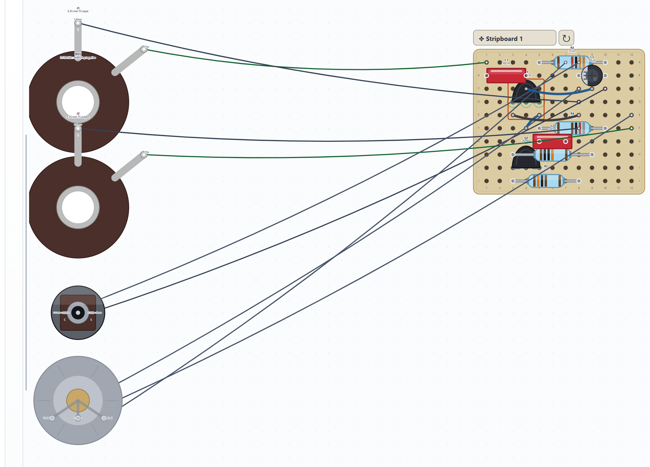
Check, repair and preserve the project
14. Run a fresh independent wiring check
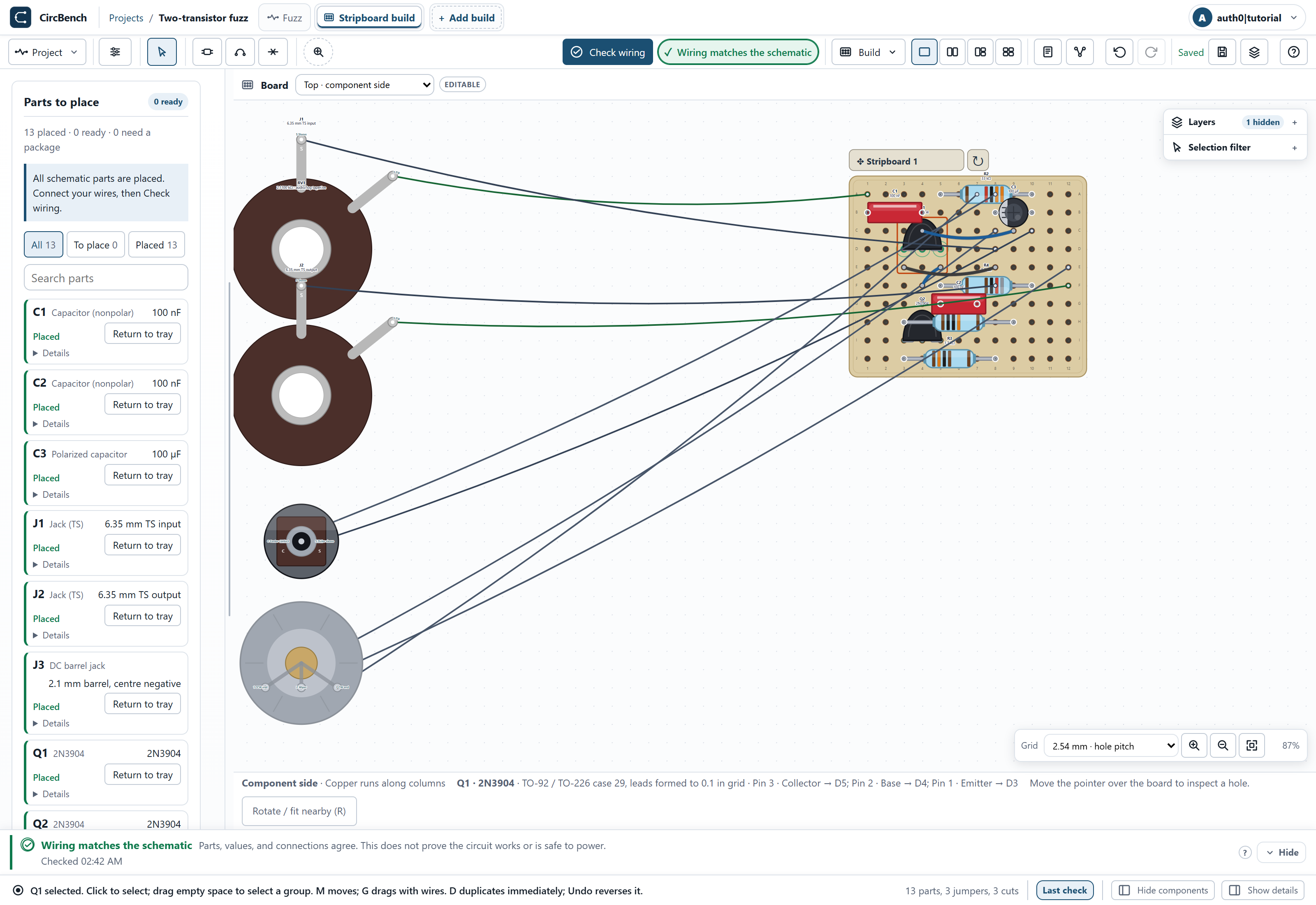
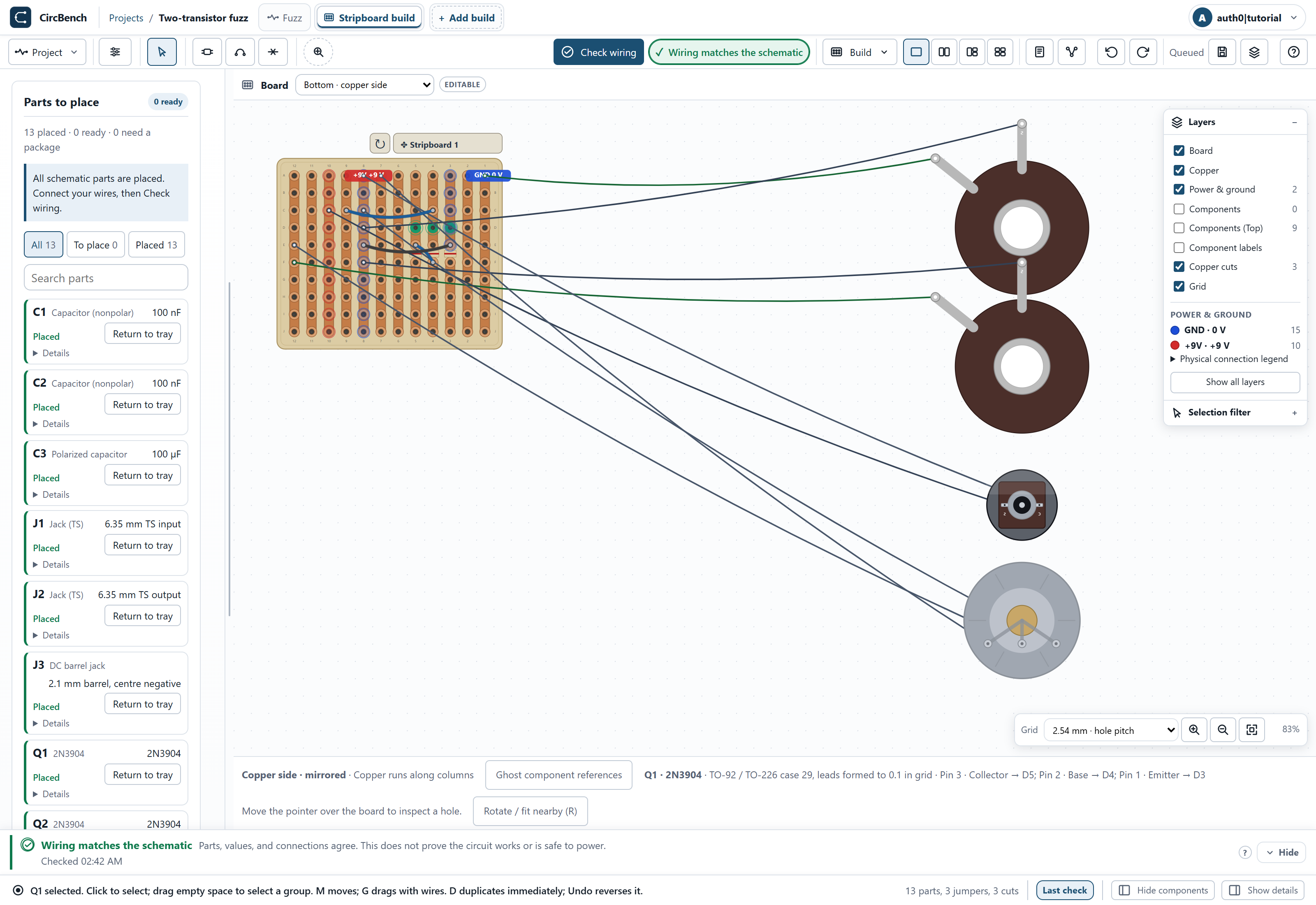
Choose Check wiring and wait for the completed match. CircBench extracts the represented board connections independently and compares them with the schematic. If your copy differs, reveal each reported open or short, verify both endpoints and check unplaced parts or fitted mappings. A previous or pending result is not a fresh match.

15. Introduce a deliberate wiring fault
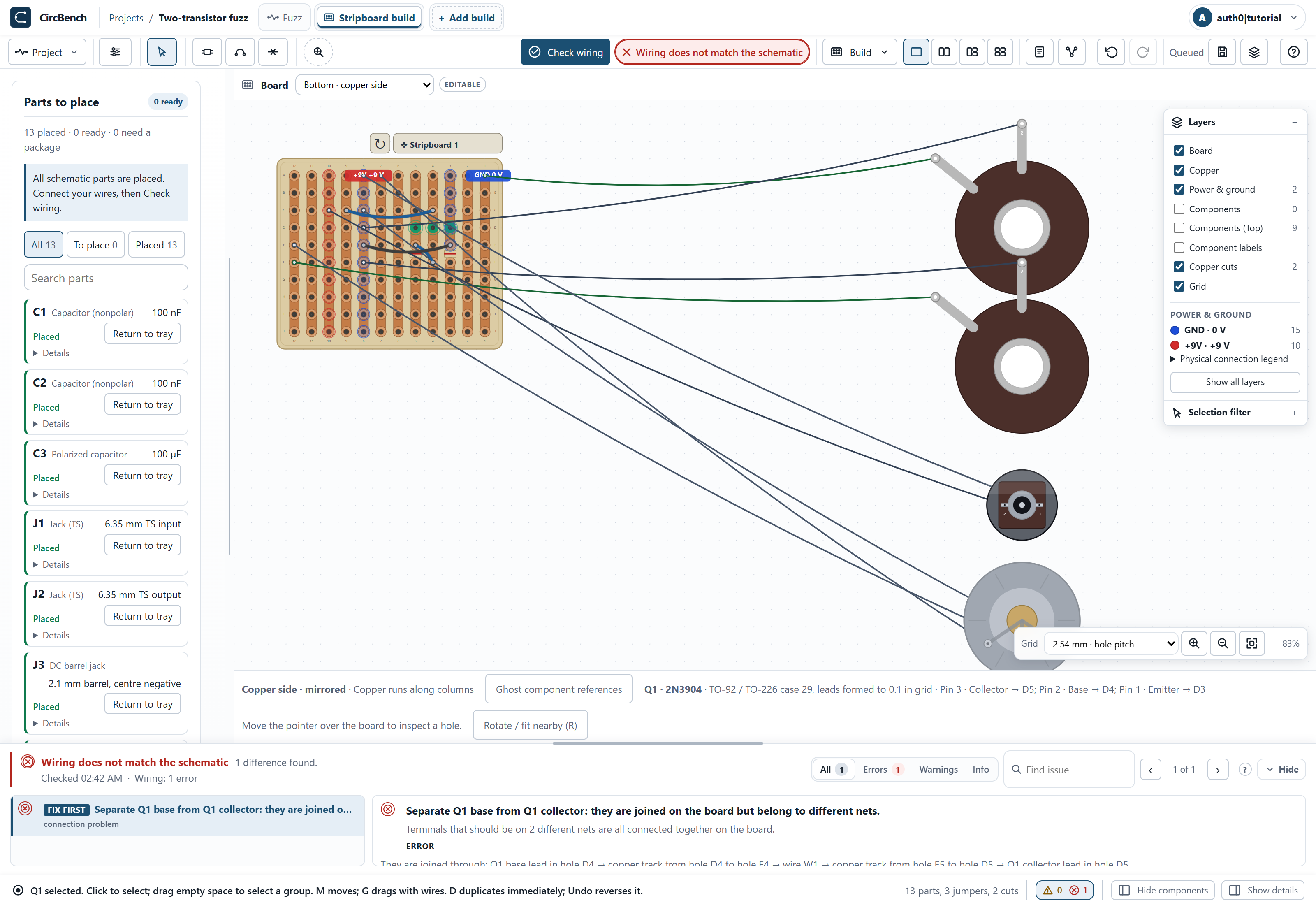
On the copper face, use Cut copper to toggle away the E4–F4 (column-4) cut, then Escape and run Check wiring. The formerly separated base regions now short through the vertical strip. Read the fresh short diagnostic and reveal its contacts. Do not substitute a visual part rotation and assume it demonstrates the same fault.

16. Undo the fault and prove the repair
Choose Undo to restore the deleted connection or cut. Run Check wiring again and wait for a fresh match. Undo alone is not verification: the completed check proves the represented topology was restored. Keep this repaired version for the following persistence and download checks.

17. Save, reload and check again
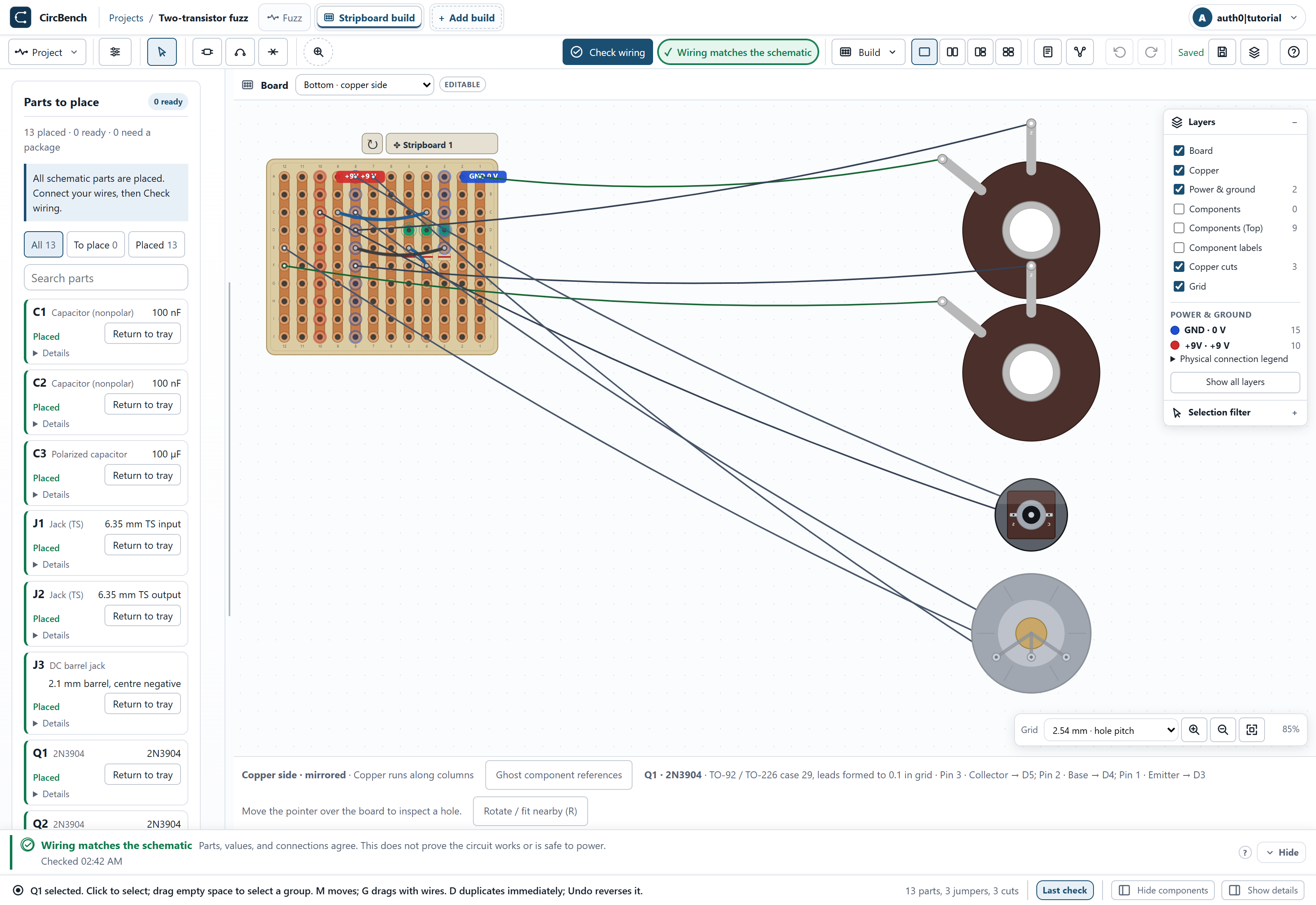
Wait for the normal save indicator, then reload the page. Open the same build and run Check wiring again. Confirm a fresh match after reload. If saving reports a problem, open save recovery and export a backup; do not assume remote account storage succeeded merely because the editor still displays the project.
18. Inspect and export the parts list
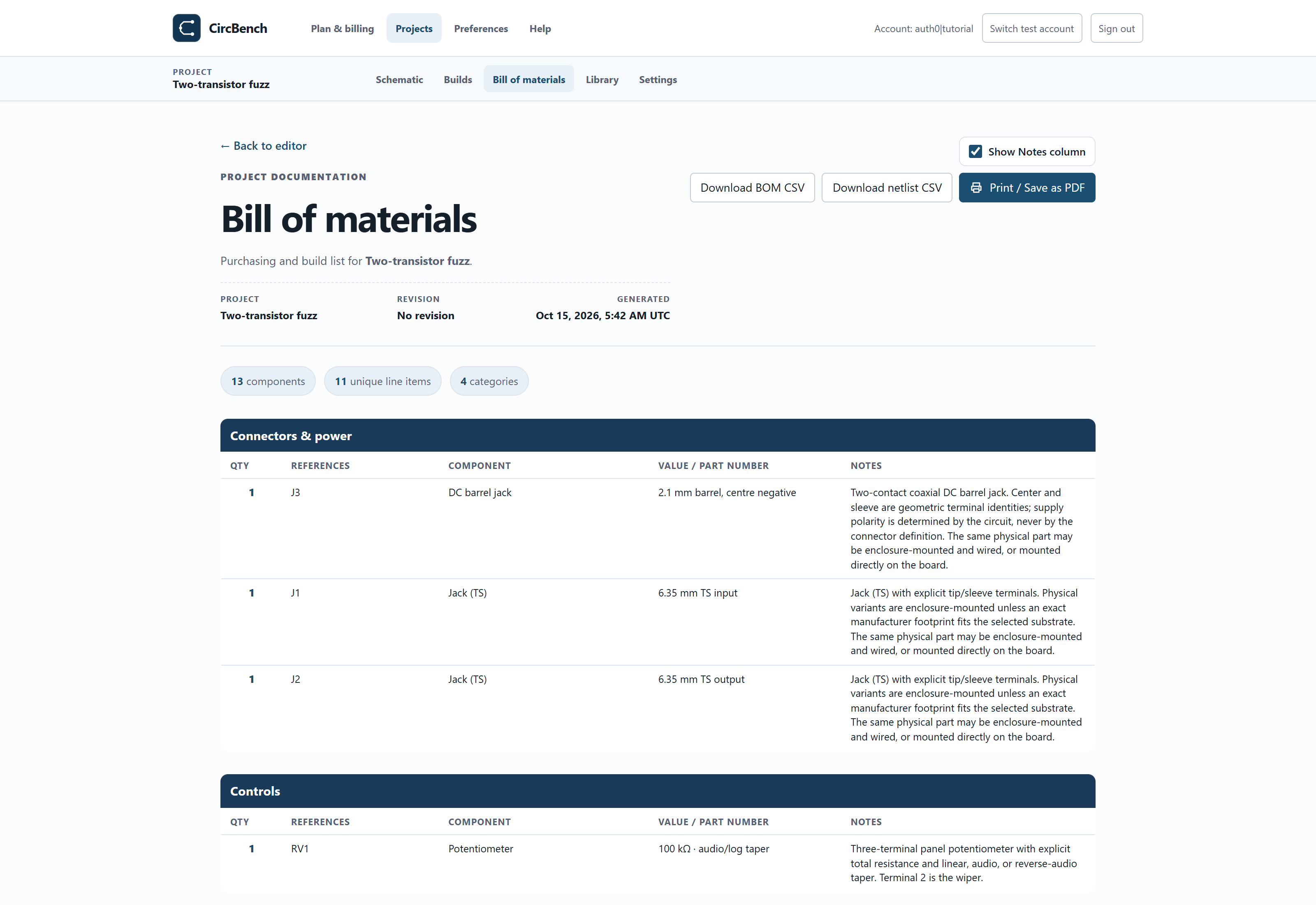
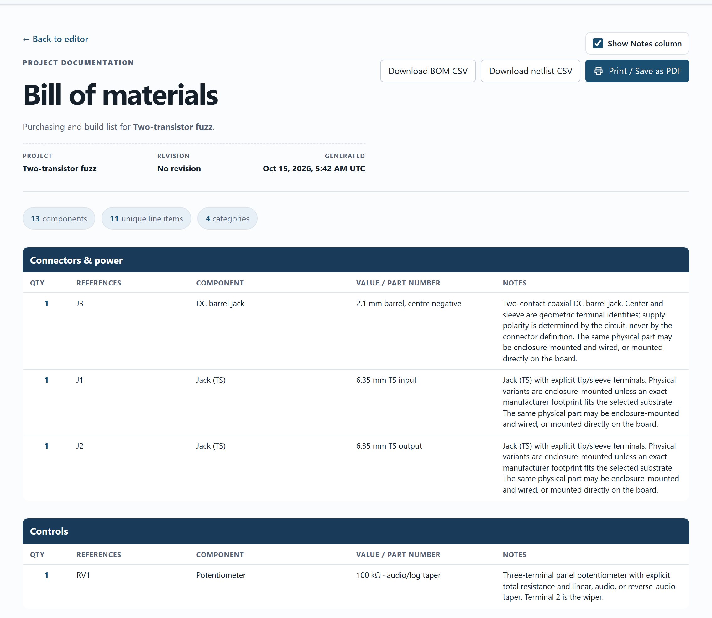
Open Bill of materials, review the fitted parts, values and quantities, then use Export CSV. Compare it with the versioned parts list above. A BOM lists represented parts; it does not select manufacturer voltage ratings or prove that a purchased package has the same terminal order. Resolve substitutions before physical assembly.
19. Export a portable project backup
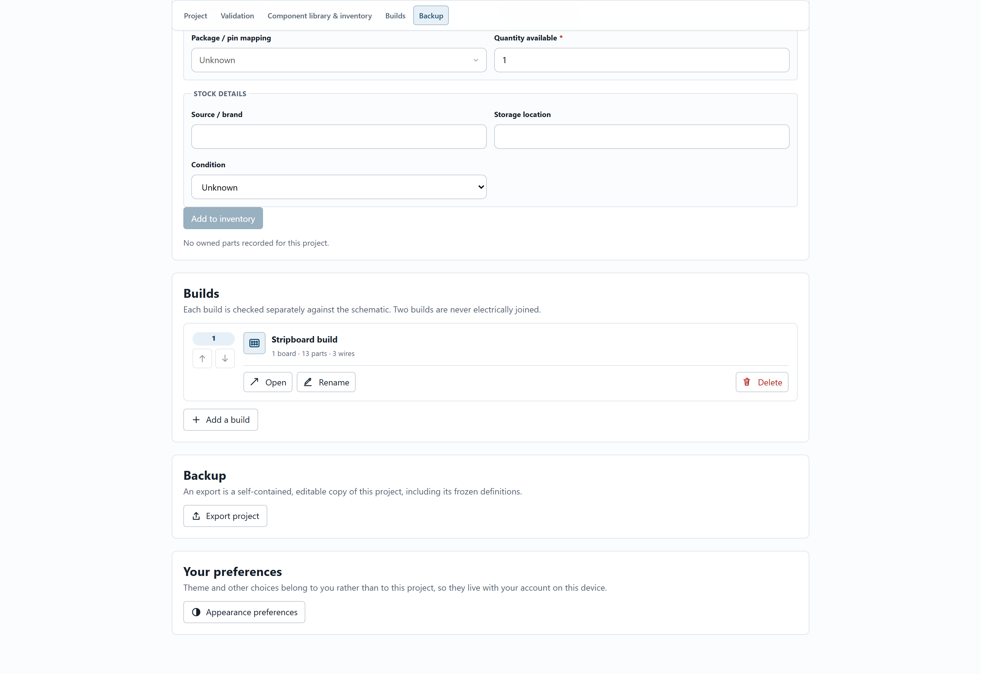
Open project Settings, go to backup and choose Export project. Keep the resulting .circbench.json file. This preserves the schematic, fitted build, definitions and saved bench/model settings. Raw simulation vectors and uploaded audio are separate outputs and are not retained in this project backup.

20. Import the backup and recheck
Return to Projects and Import the backup file. The imported copy appears in your library; explicitly Open its schematic, then its build. Run Check wiring and confirm a new match. If an import is rejected, keep the original file and compare its schema/version with the app rather than editing integrity fields by hand.
What this result establishes
This is a CircBench-authored nominal silicon fuzz lesson, not a measured vintage pedal clone. Device spread, component tolerances, noise, ratings, temperature effects and physical construction quality require separate evaluation. A wiring match only compares the represented connectivity.
The screenshots show current solver results and fresh wiring checks for this exact example version. They do not assert that hardware was assembled, measured or qualified. Use the supplied source, load and stimulus settings when comparing results.
CircBench authors the schematic, v2 bias revision and independent vertical-strip layout. The versioned project and full BOM below preserve the exact 1.3 kΩ R3 circuit used in these screenshots.
Your next project
Compare this coupled-transistor behavior with the explicit diode network in the Electra-style distortion guide.