perfboard · intermediate
Build an Electra-style silicon distortion on perfboard
Draw a transistor and antiparallel-diode distortion, compare bias and clipping, and follow a checked perfboard layout with clear screenshots and downloads.
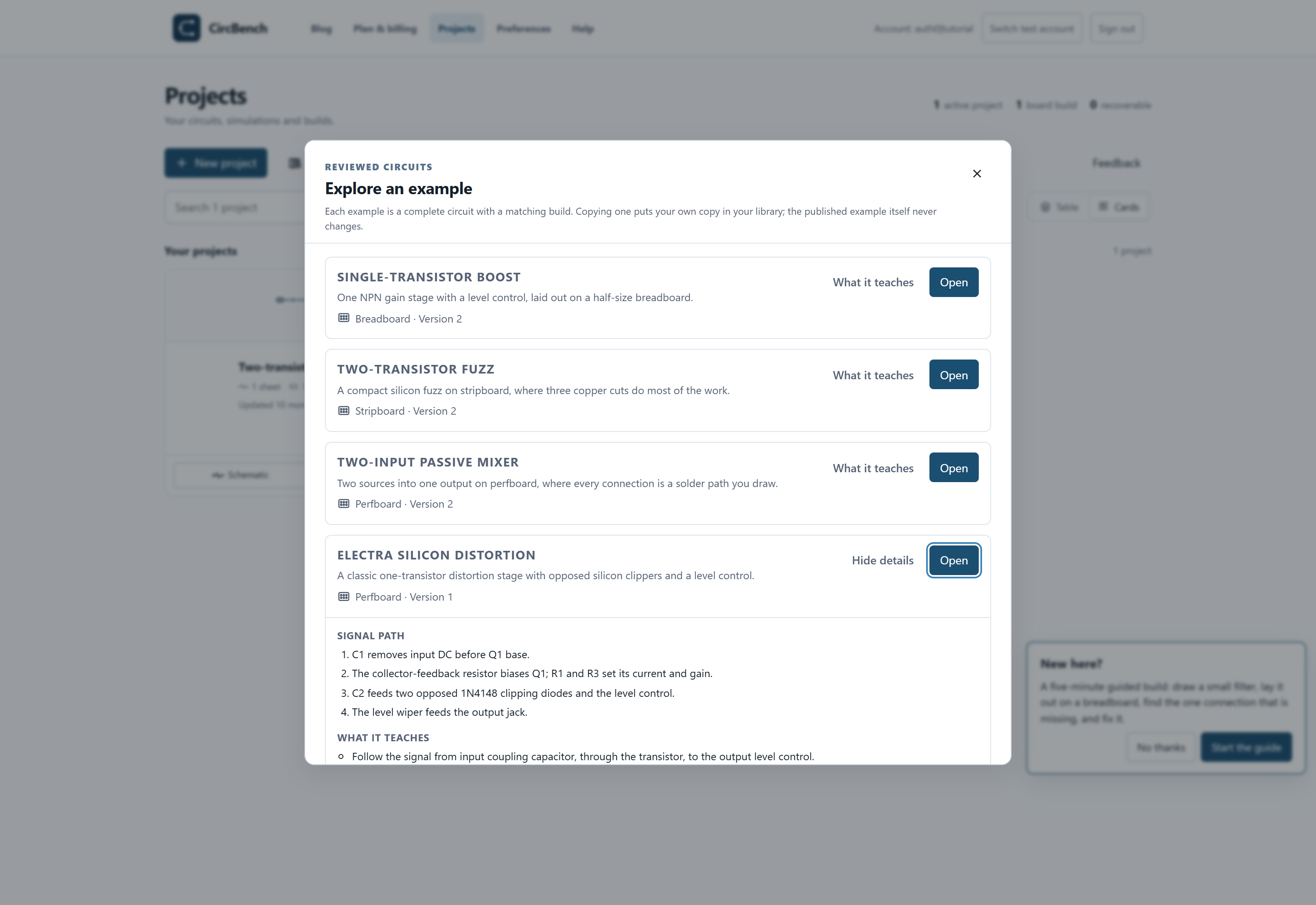
The app opens the current example chooser. Choose Open to create your own account copy. For this guide's exact v1, download and import the project backup if the catalog version has changed.
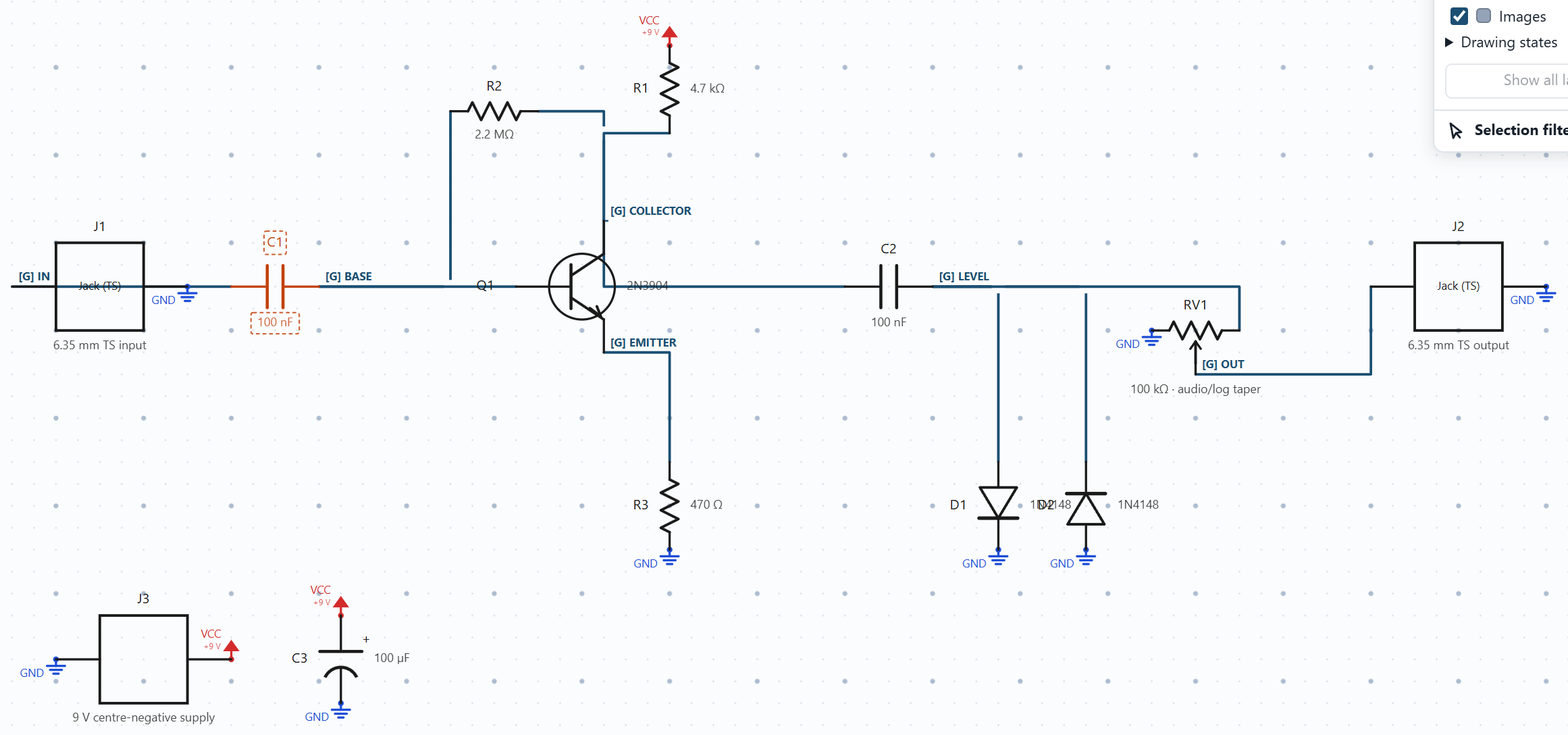
This Electra-style silicon variant separates transistor amplification from an explicit diode clipping network. You will trace both parts, compare small-signal and driven results, and inspect a complete 16 × 17 perfboard layout. The example adapts the documented topology rather than claiming an original invention or an exact historical clone.
Parts: Q1 2N3904; R1 4.7 kΩ, R2 2.2 MΩ, R3 470 Ω; C1/C2 100 nF; opposed D1/D2 1N4148; A100K level pot; C3 100 µF supply filter; panel audio/DC hardware.
Before starting: have a CircBench account and use a copy for experiments. This is a software build and simulation walkthrough; the images are actual application screenshots, not photographs of assembled hardware. Every numbered step has a detail image and a link to its unmodified full context PNG. Open full size when comparing small pin labels, especially on a phone.
Draw and understand the schematic
1. Open the exact reviewed example
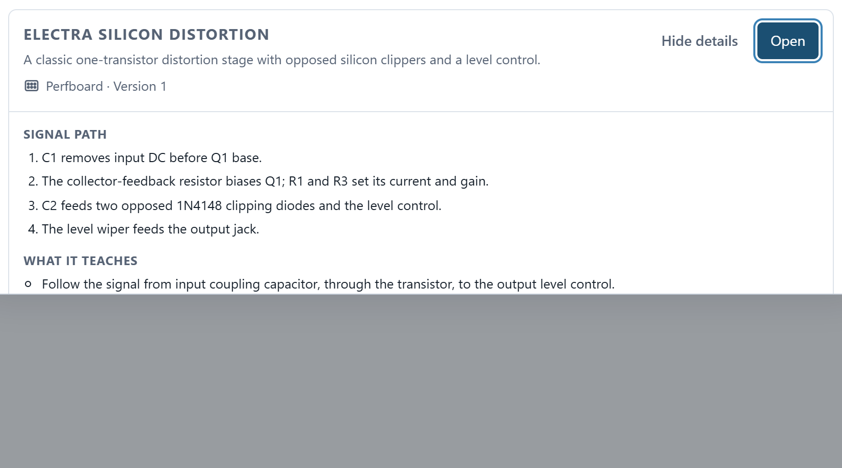
Use the example link above, sign in if requested, and confirm Electra silicon distortion, version 1 in Explore an example. Choose Open to create your own account copy. The link alone does not create a project. If the catalog changes, import the versioned backup above to follow this precise guide. All screenshots show the actual reviewed copy, with completed wiring as a reference for your own drawing.
2. Start with the common-emitter stage
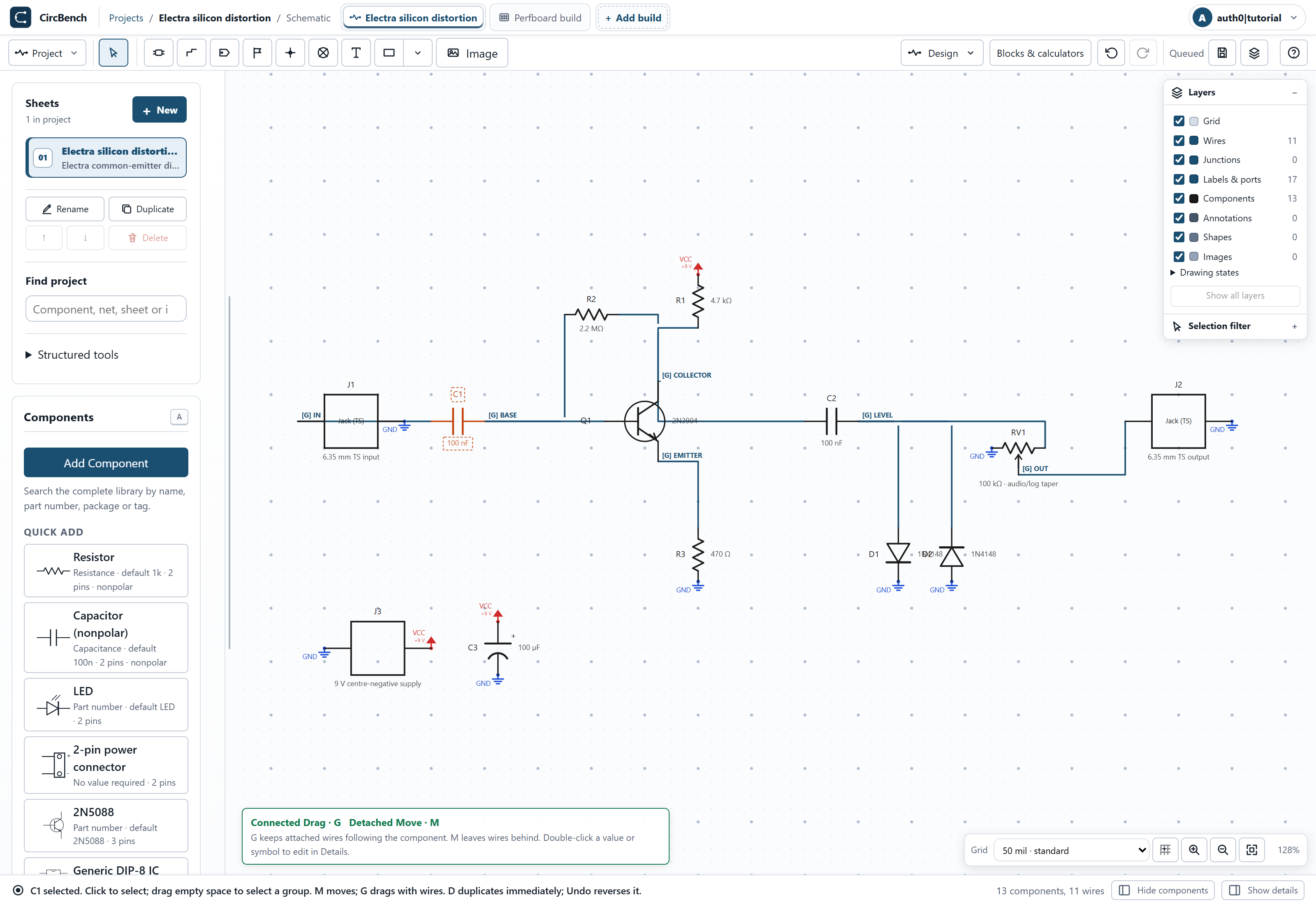
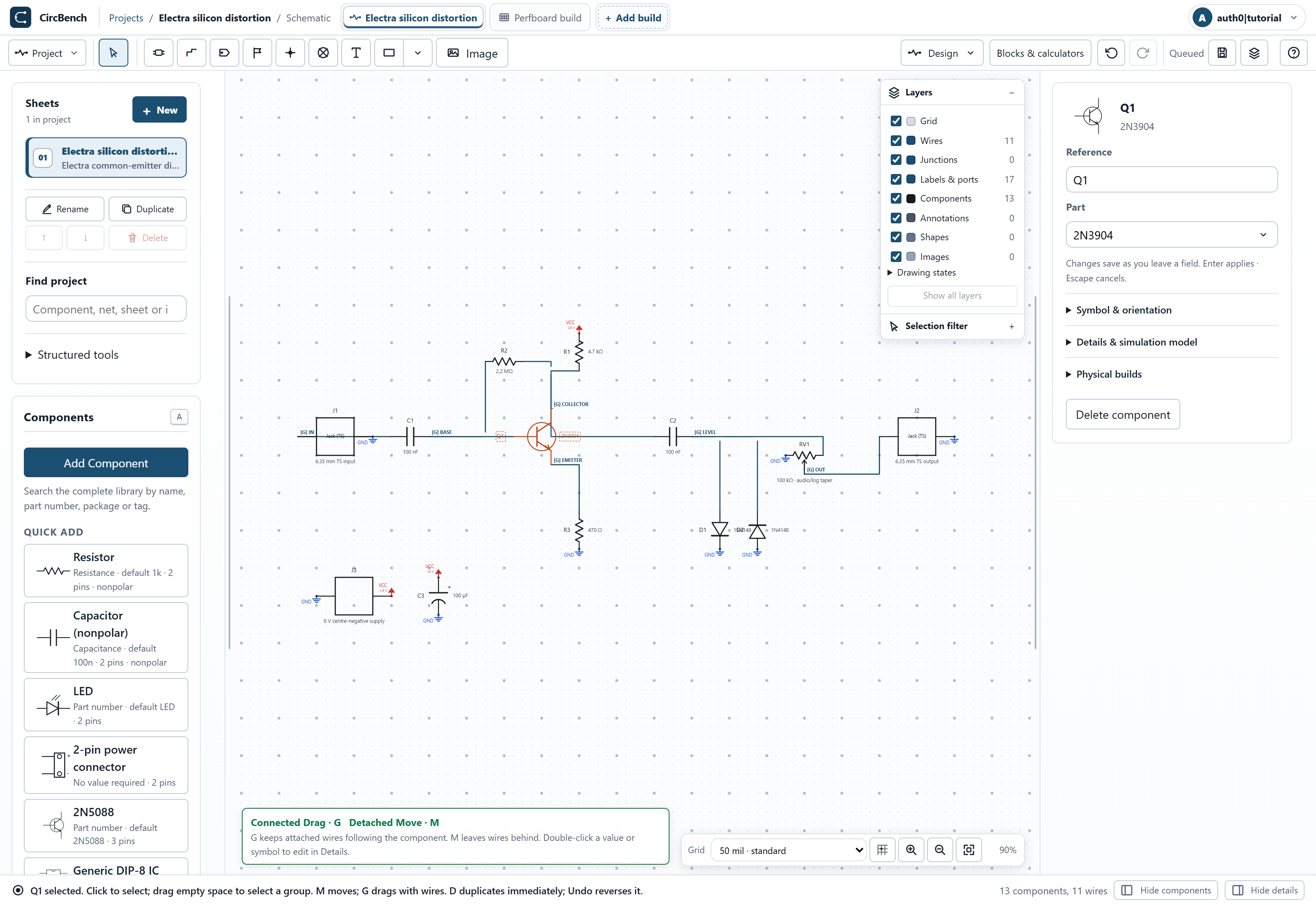
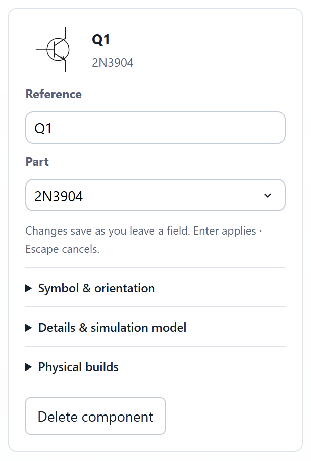
Inspect Q1 and identify E, B and C. Draw R1, 4.7 kΩ, from 9 V to collector; R2, 2.2 MΩ, from collector to base; and R3, 470 Ω, from emitter to return. These establish the transistor’s DC paths before the diode network is added. Verify the selected device instead of inferring pins from a package outline.
3. Add the two coupling capacitors
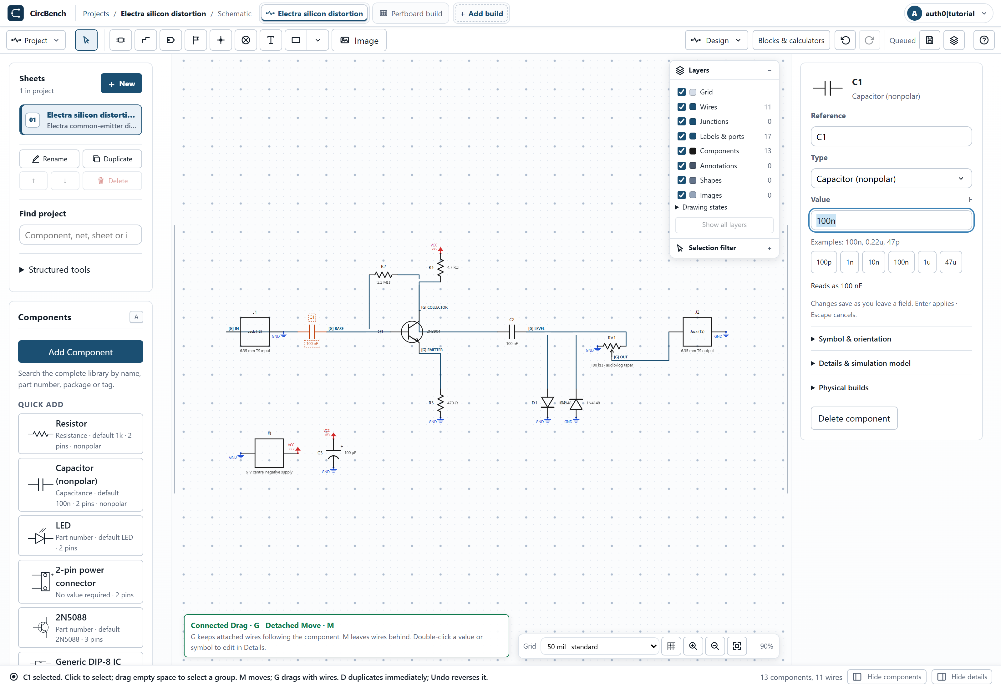
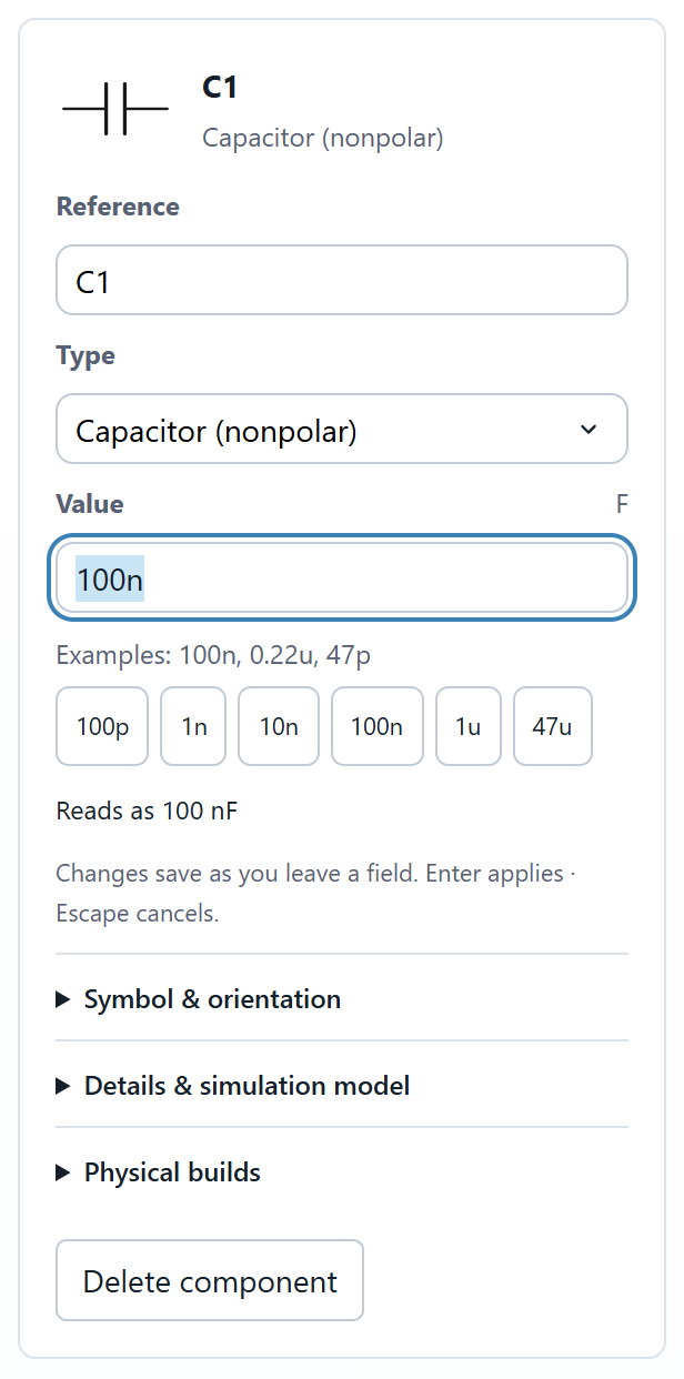
Inspect C1 and confirm 100 nF. Connect it between input and base, then add C2, also 100 nF, from collector to the clipping/output node. Keeping the diode pair after C2 separates its return path from collector DC bias. The two coupling capacitors are nonpolar in this reviewed fit.
4. Oppose the diodes and complete the drawing
Fit the full schematic. Connect D1 and D2 antiparallel between the post-C2 signal and return: one anode faces the signal and the other cathode faces it. Identify both K terminals. Add the level track, wiper-to-output connection and 100 µF supply filter. This variant uses 1N4148 silicon approximations and an authored level/filter arrangement.
Configure and interpret the simulation
5. Configure explicit supply and approximations
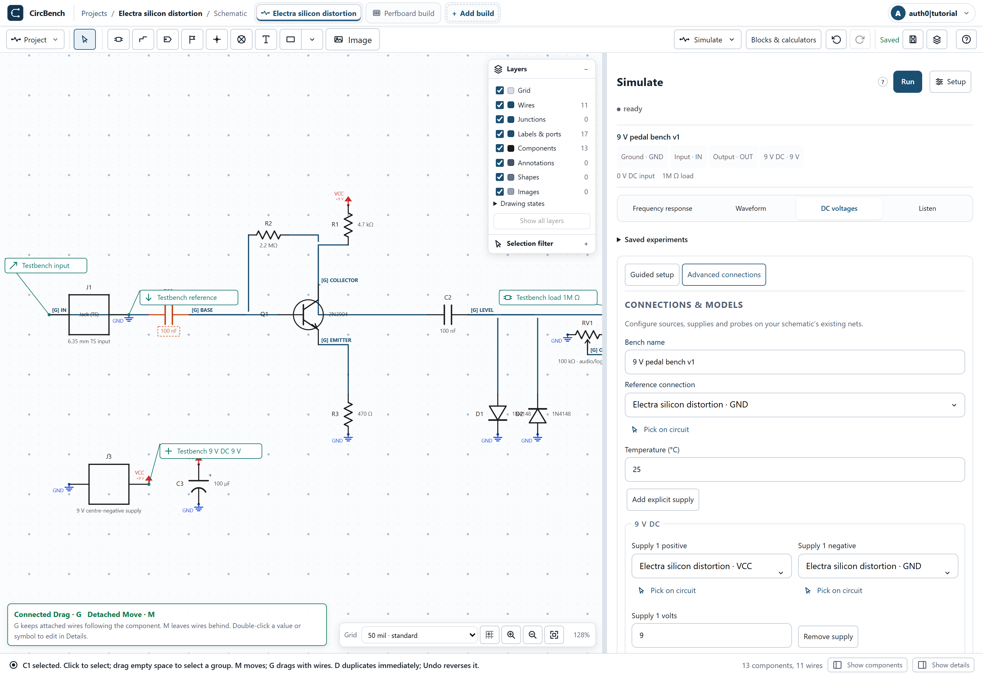
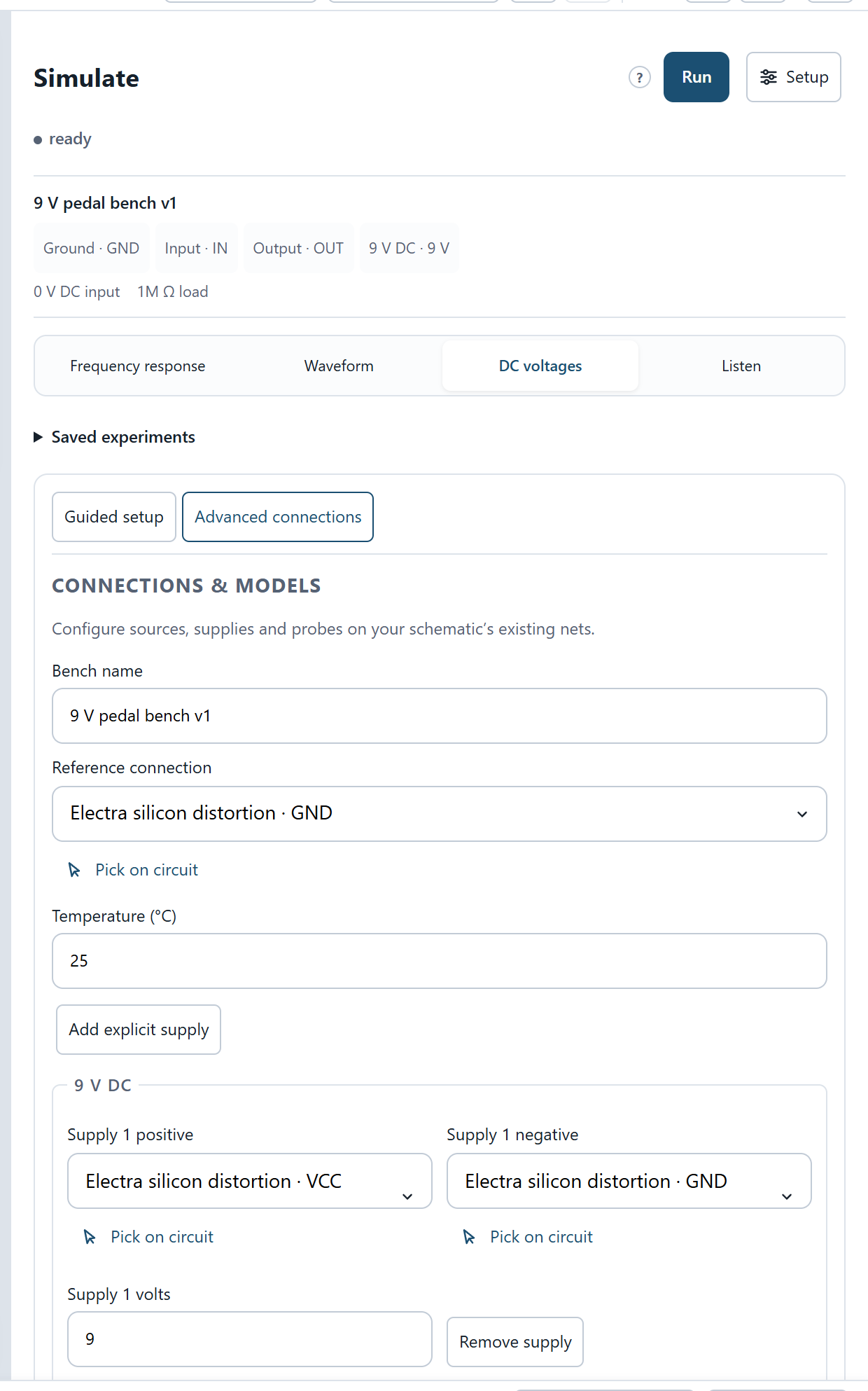
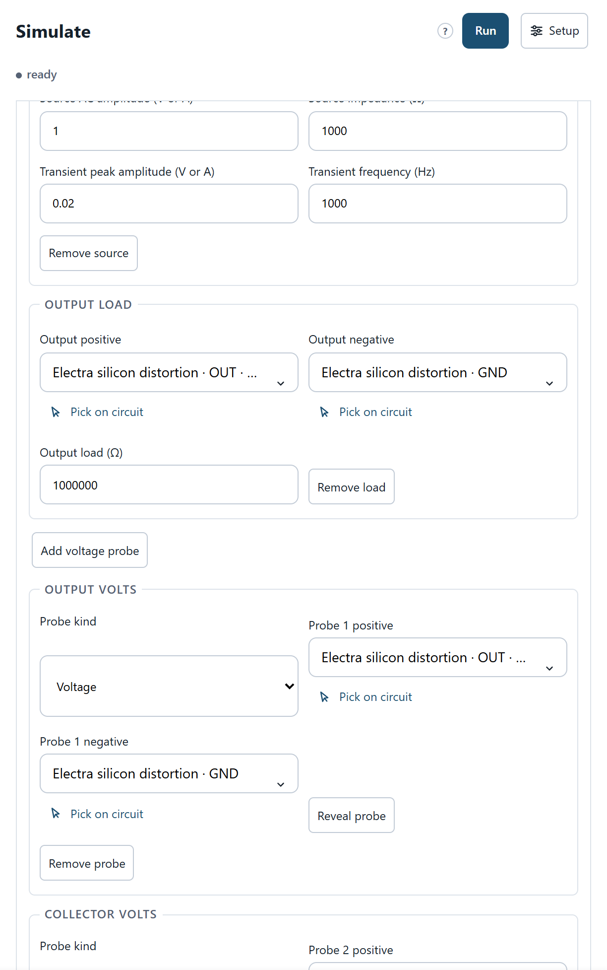
Choose Simulate → Setup. Keep 9 V, 1 kΩ source, 1 MΩ load, full level, 25 °C and the authored 20 mV-peak 1 kHz sine. Verify input/output/reference endpoints and deliberately select reviewed active-device approximations. Save setup and selected models. Both transistor and diode behavior depend on these nominal model choices.
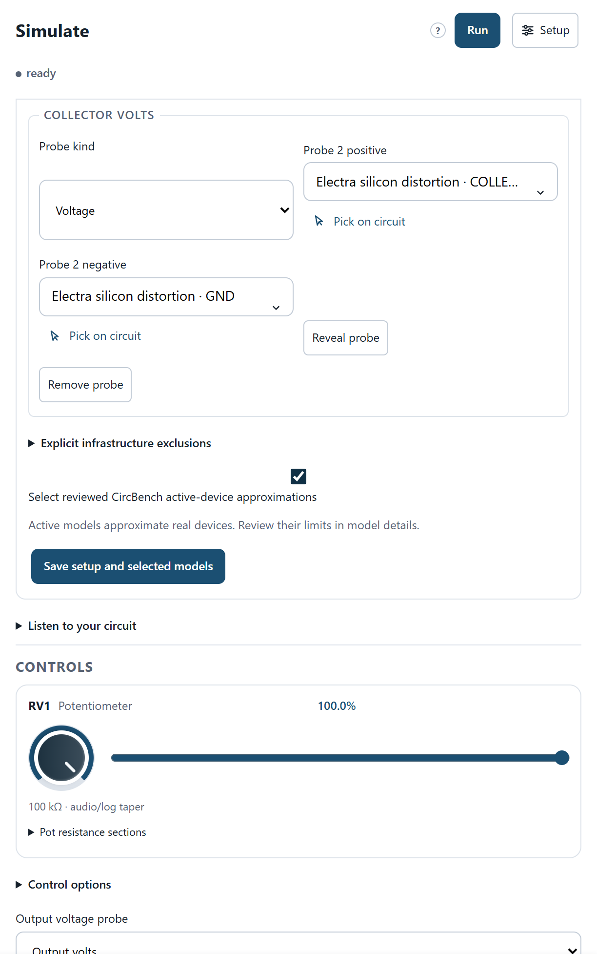
6. Inspect collector operating voltage
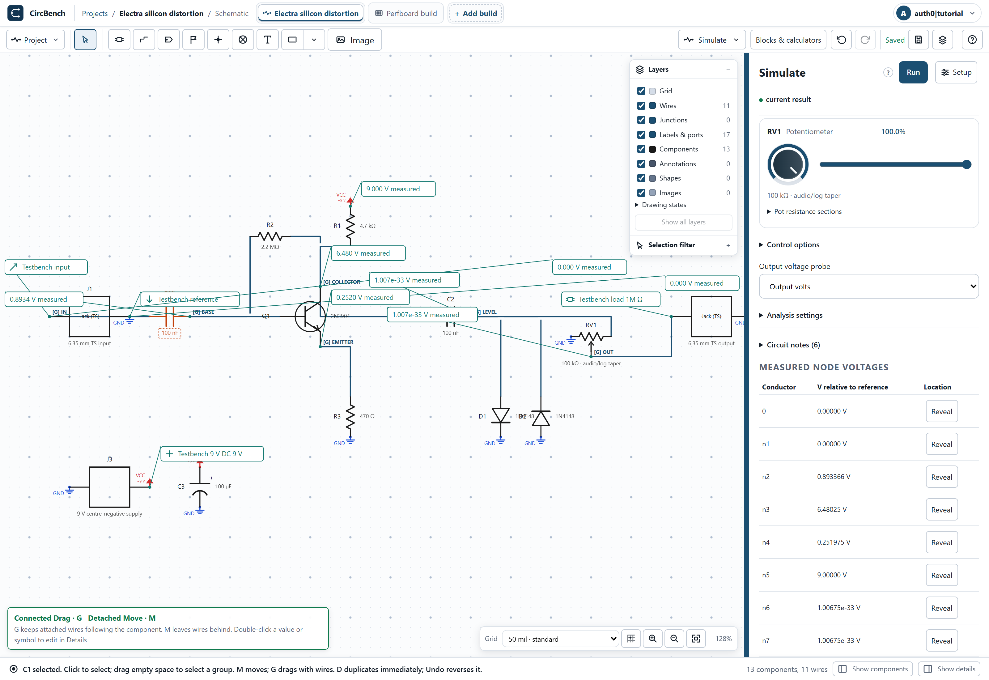
Run DC operating point and wait for current result. Reveal the collector node; this captured nominal bench places it around 6.48 V. Inspect base and emitter as well. An off-center collector voltage constrains the available swing. If your result differs, compare supply, resistor values, model selection and exact v1 circuit before comparing waveform shapes.
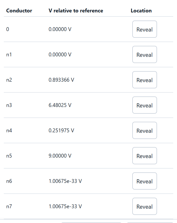
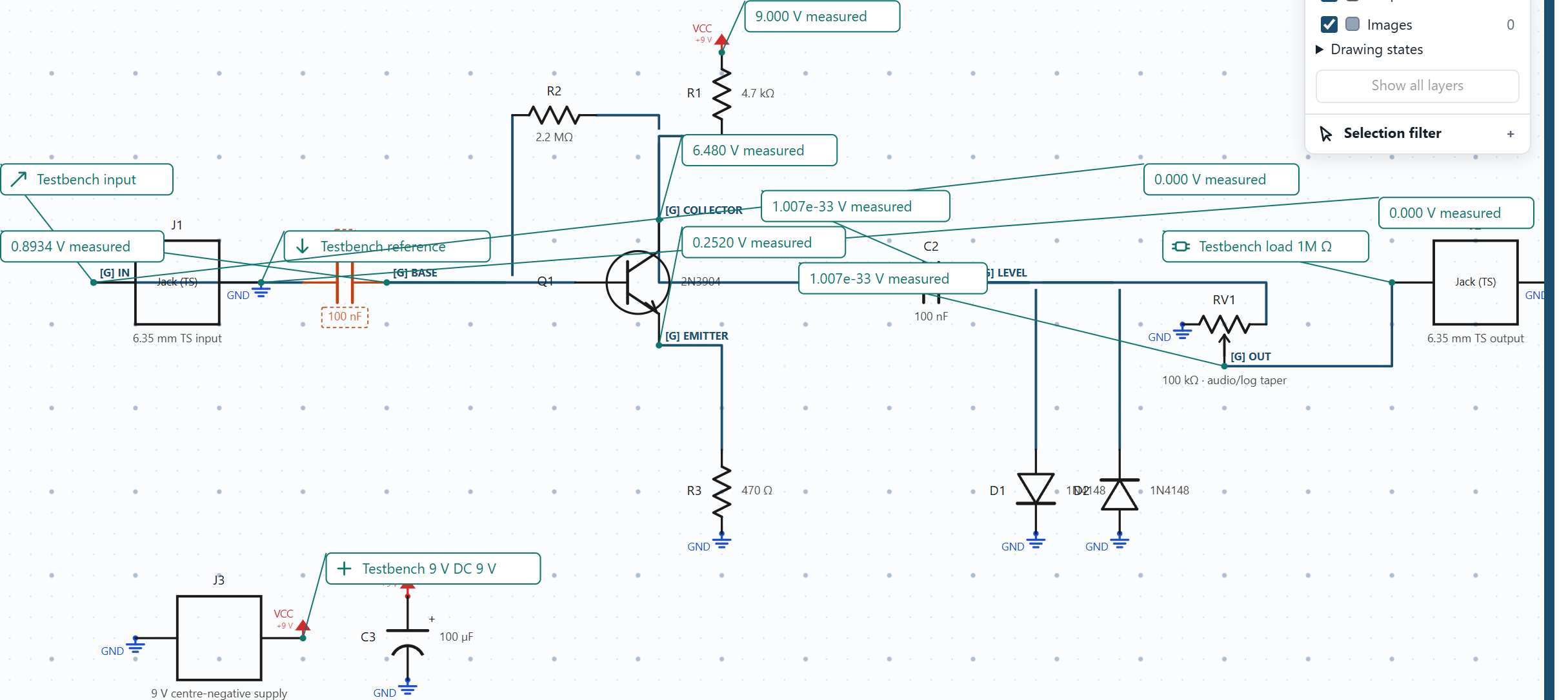
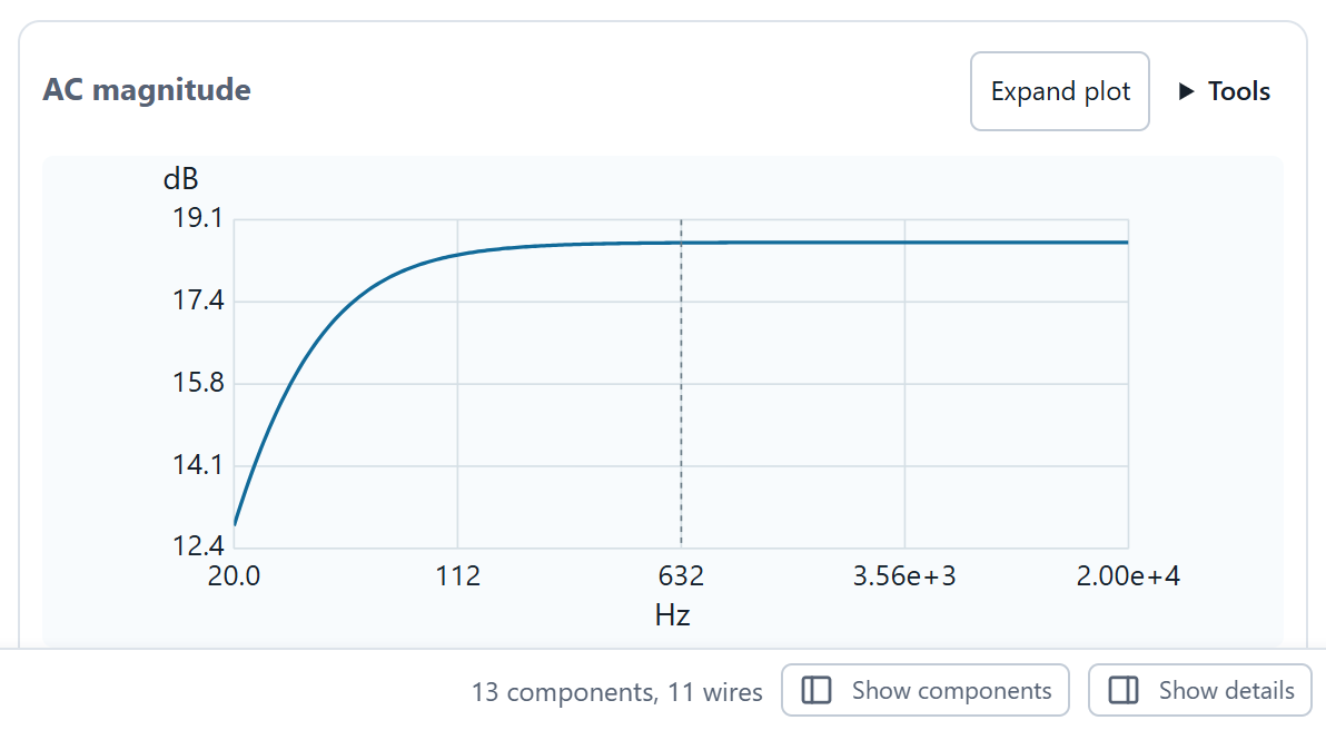
7. Inspect the linearized response
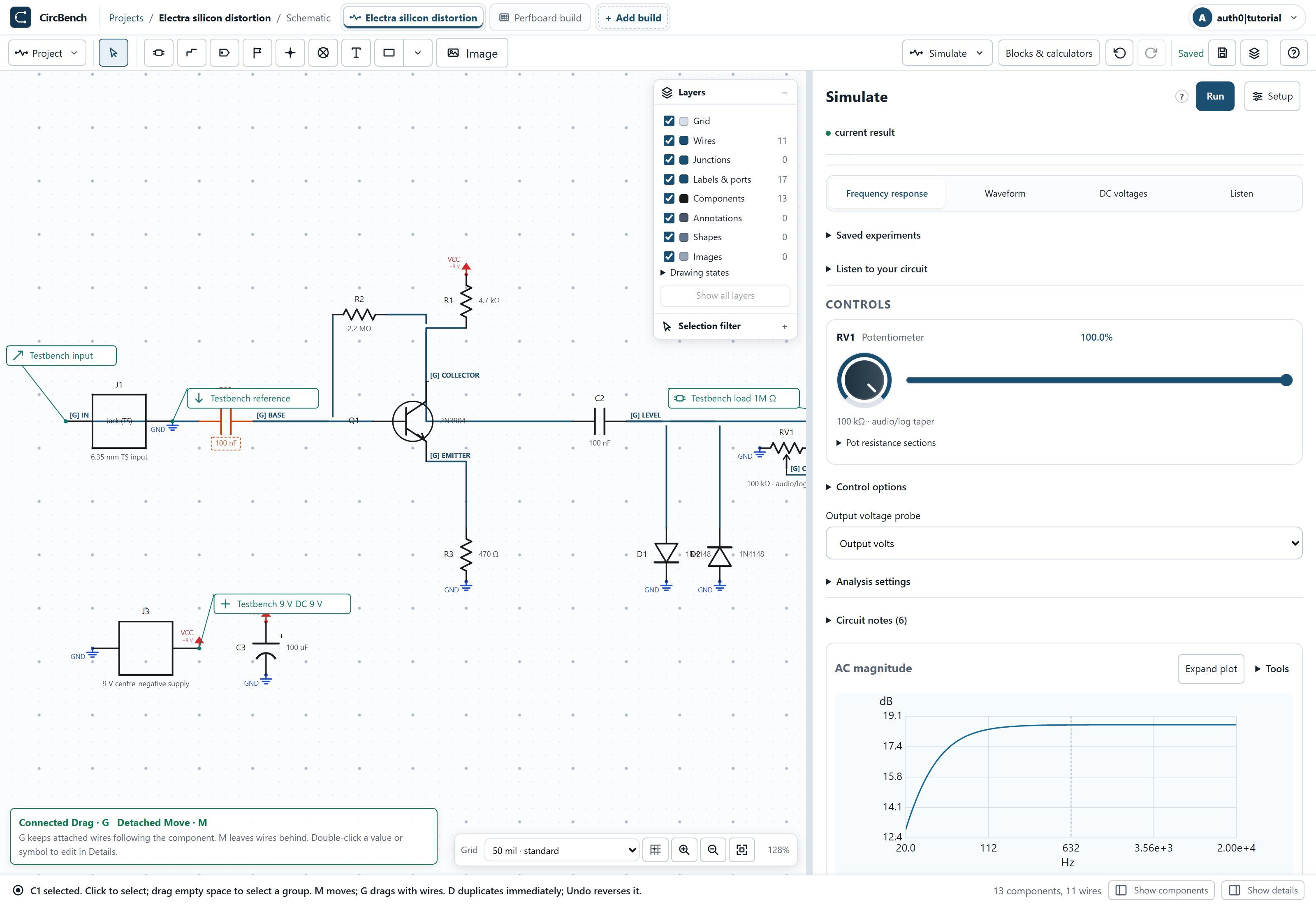
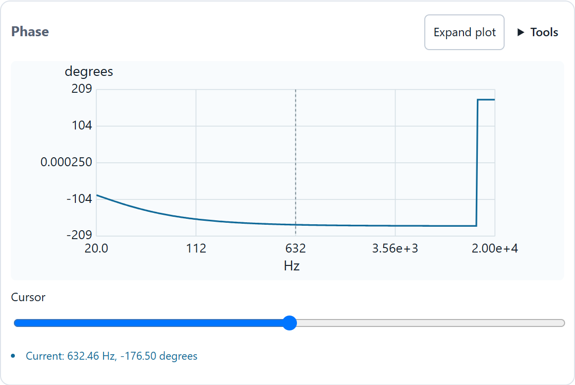
Run AC frequency response from 20 Hz to 20 kHz. Read gain in dB and phase in degrees in the separate images. This response is computed around the DC point with small perturbations. It helps explain bandwidth and stage gain, but cannot by itself tell you the driven diode-limited waveform.
8. Run the authored 20 mV waveform
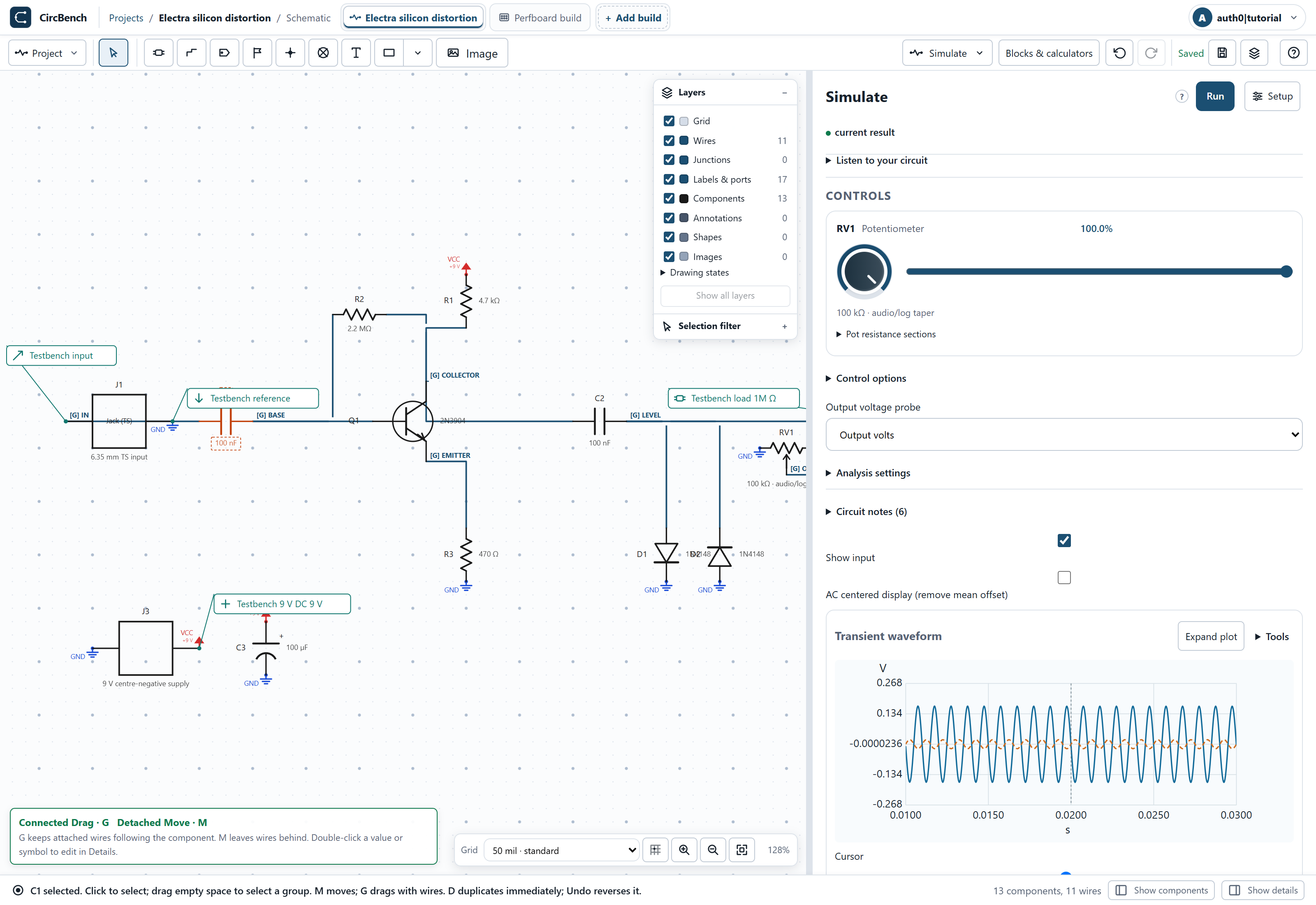
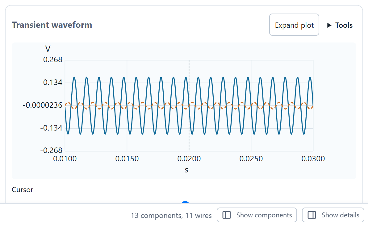
Choose Transient waveform and run the 0.02 V-peak 1 kHz bench. Compare the solid output with dashed input over settled cycles. Note amplification and inversion under the stated load. The diode pair’s effect depends on instantaneous current and the selected approximation; it is not a universal hard 0.7 V switch.
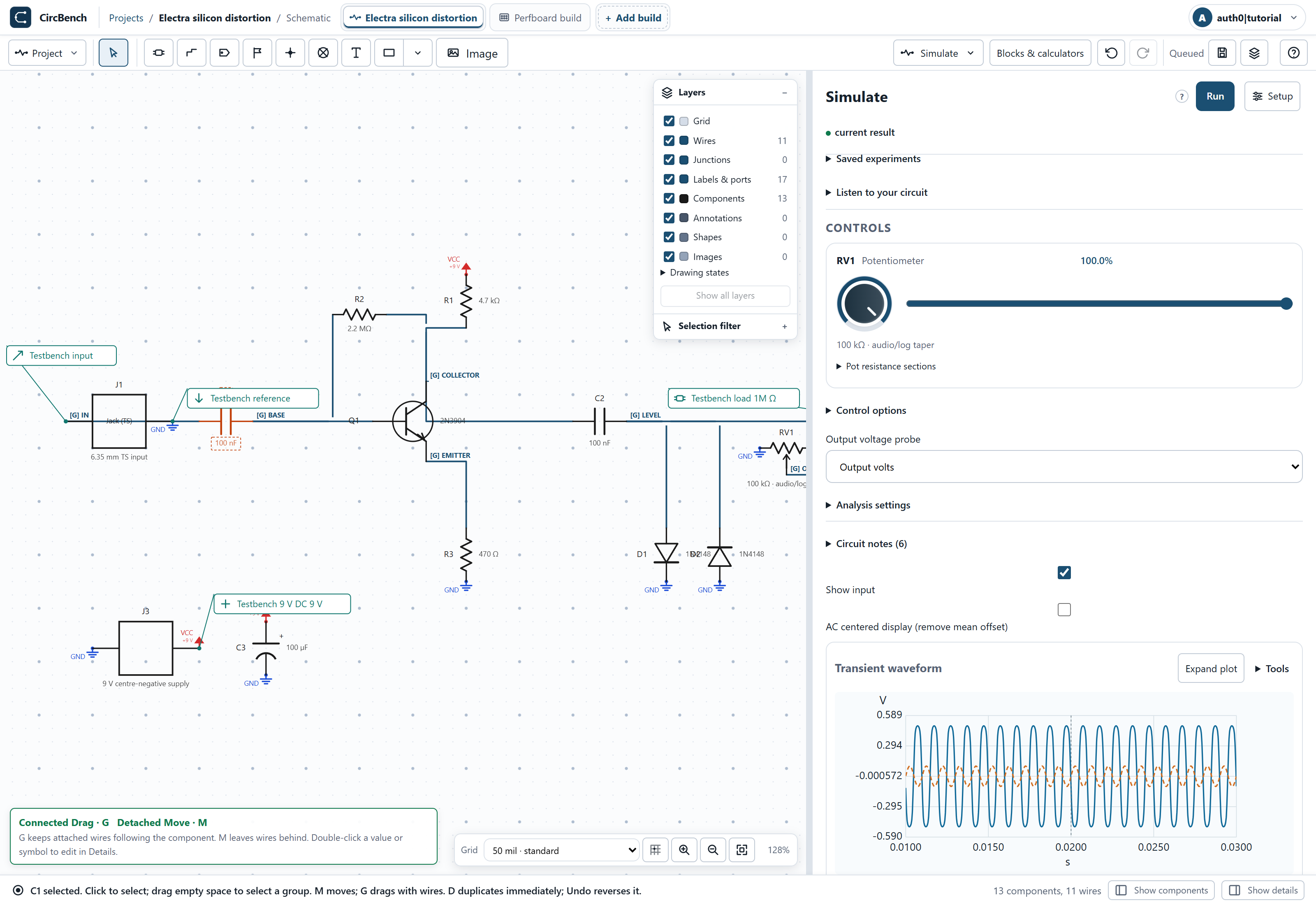
9. Increase drive to inspect clipping
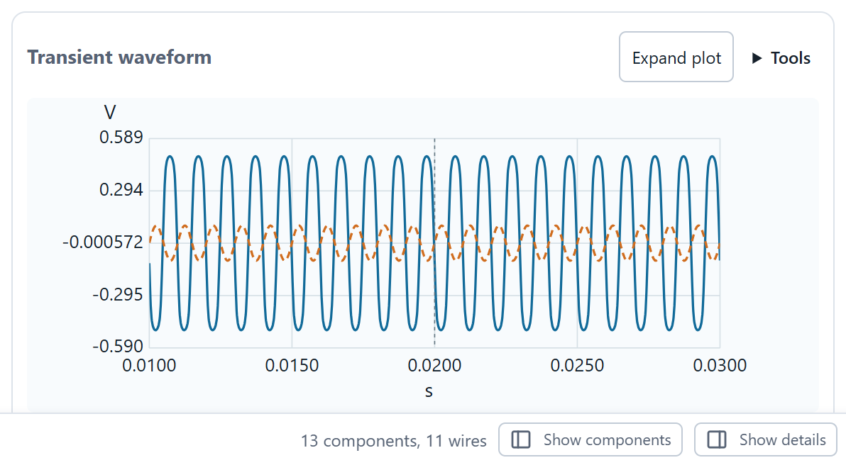
Change Transient peak amplitude to 0.1 V in Setup, save and run a new waveform. Compare the changed peaks with the 0.02 V case while holding level and terminations fixed. Describe the captured shape rather than assigning a generic clipping voltage. Restore 0.02 V and save before the board walkthrough; rerun for a current restored result.
Build the physical layout
10. Orient the reviewed perfboard
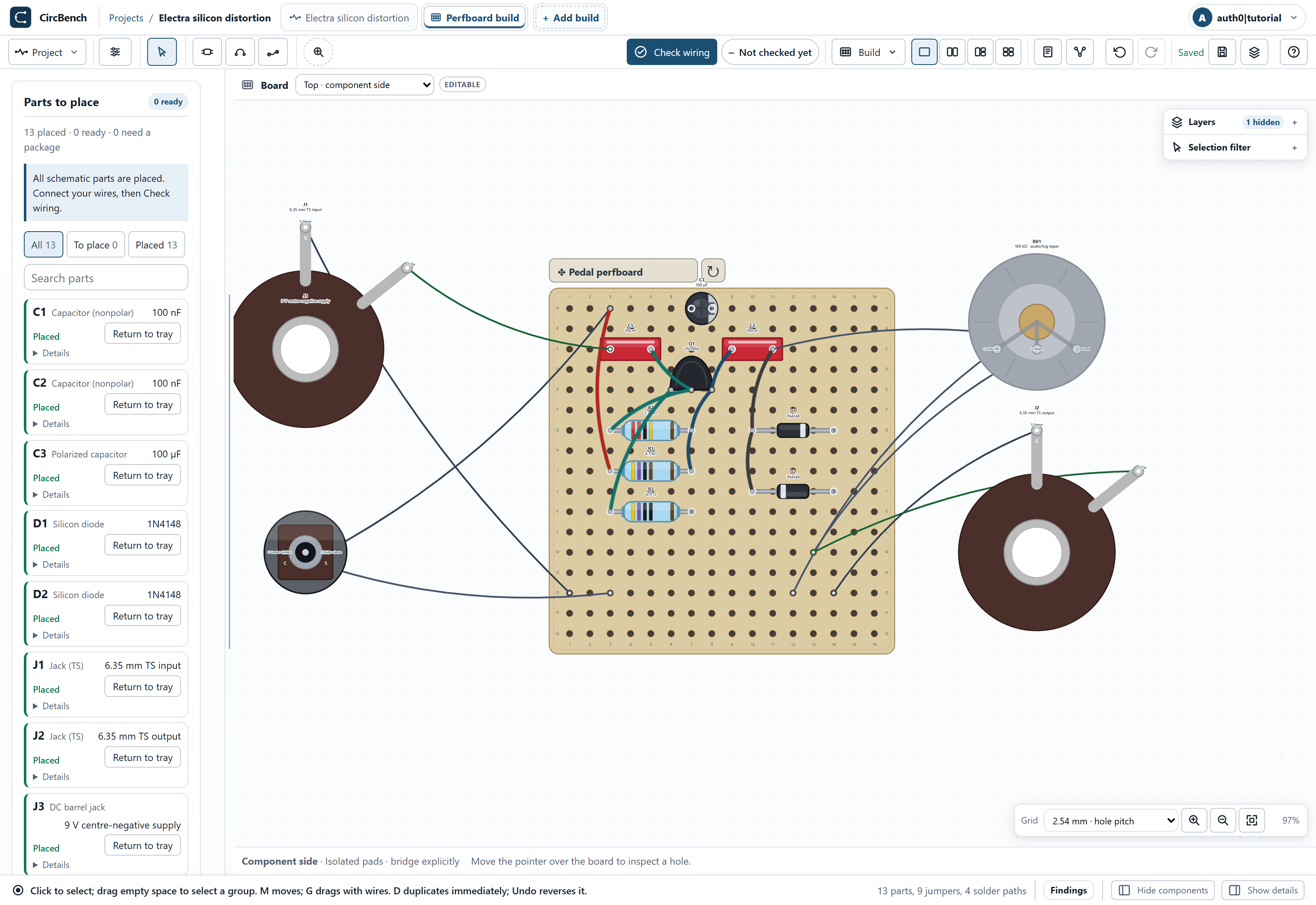
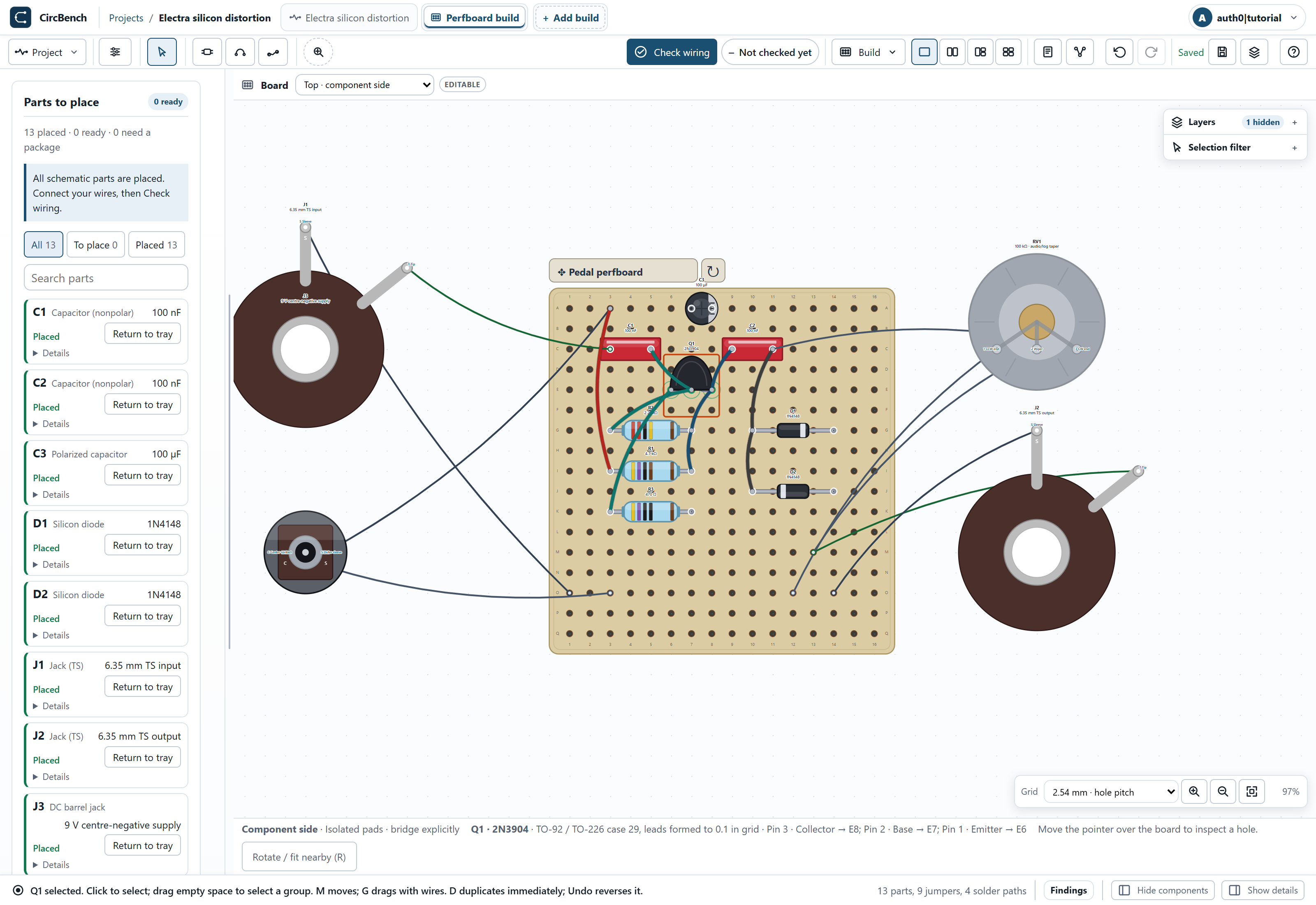
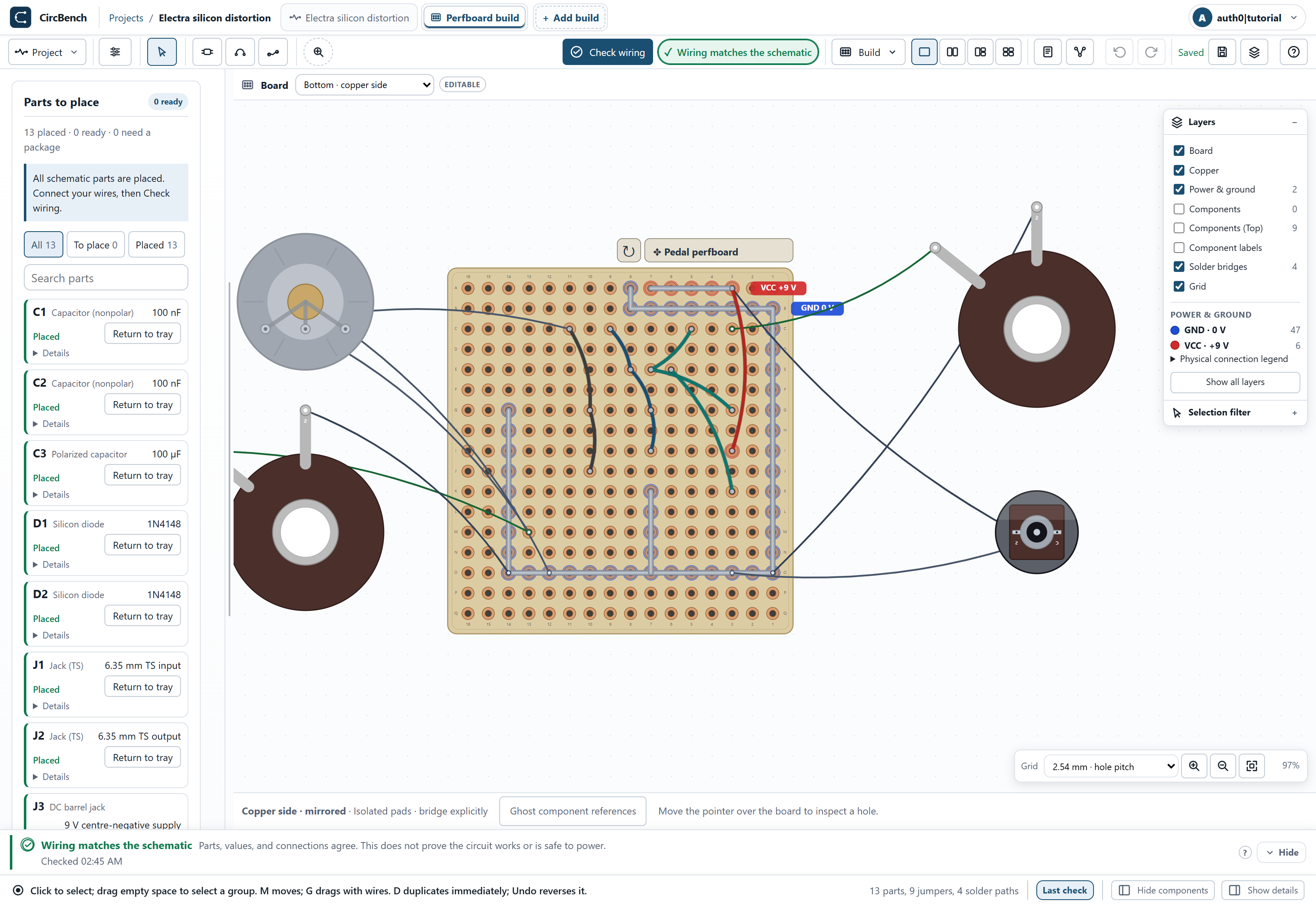
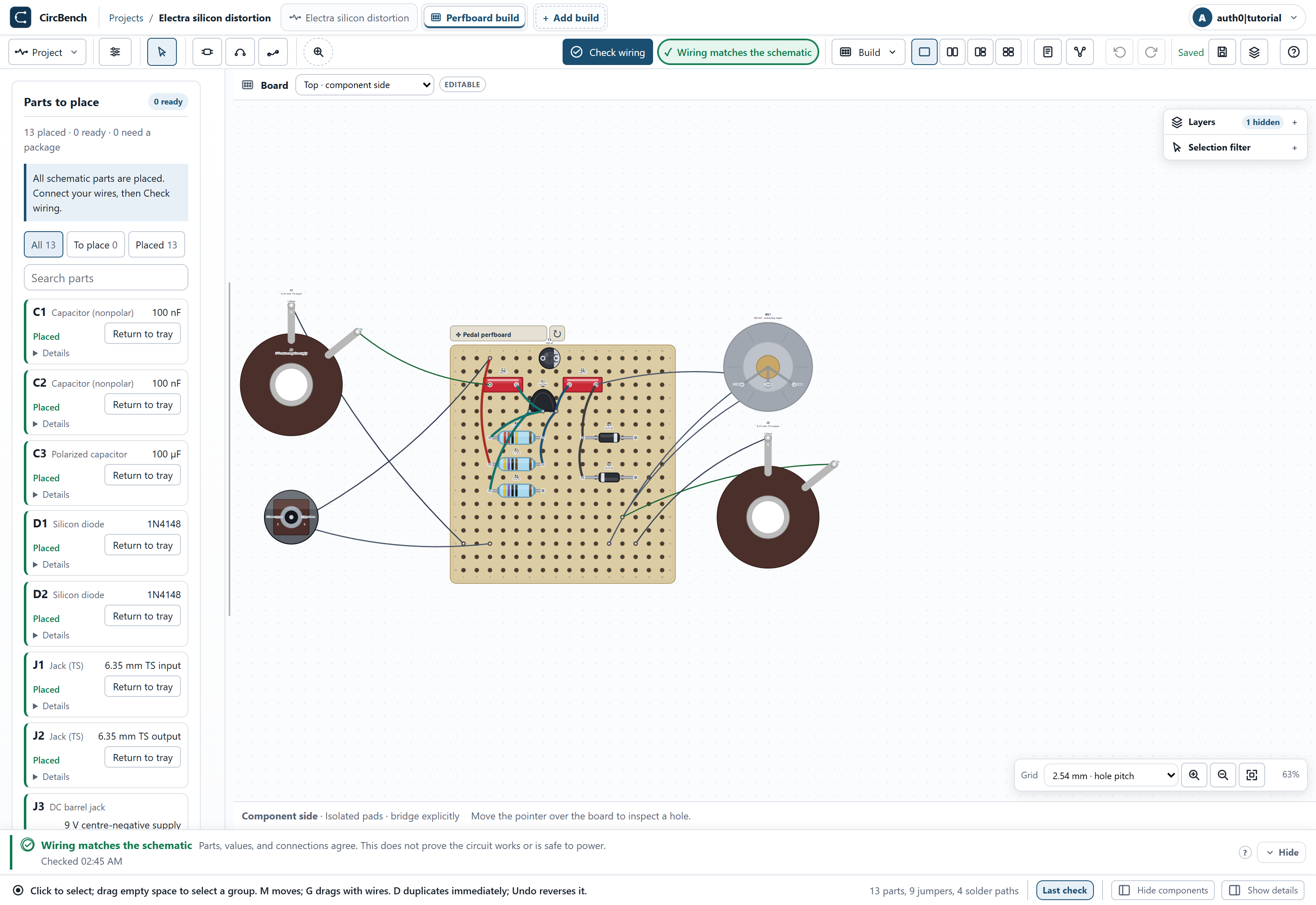
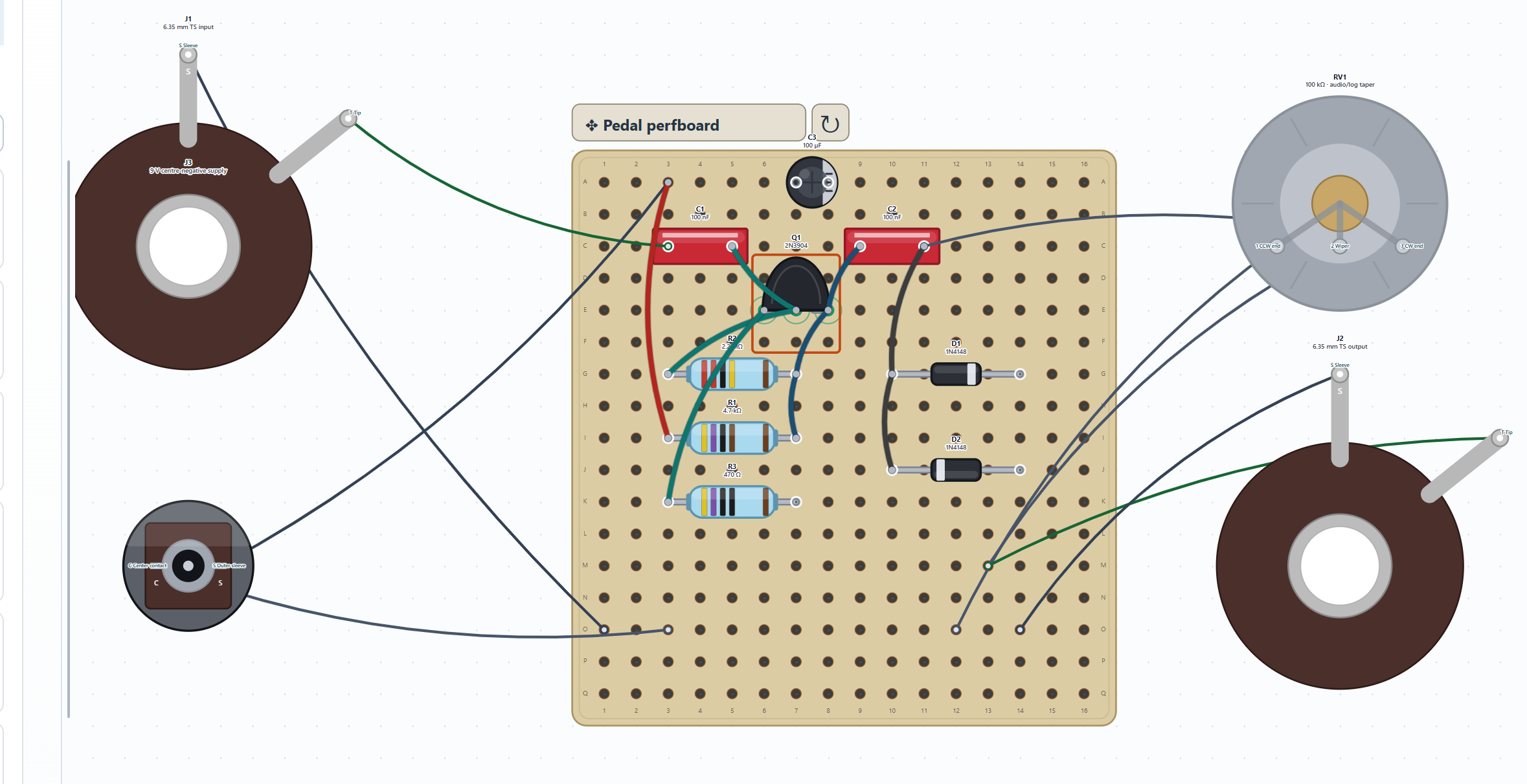
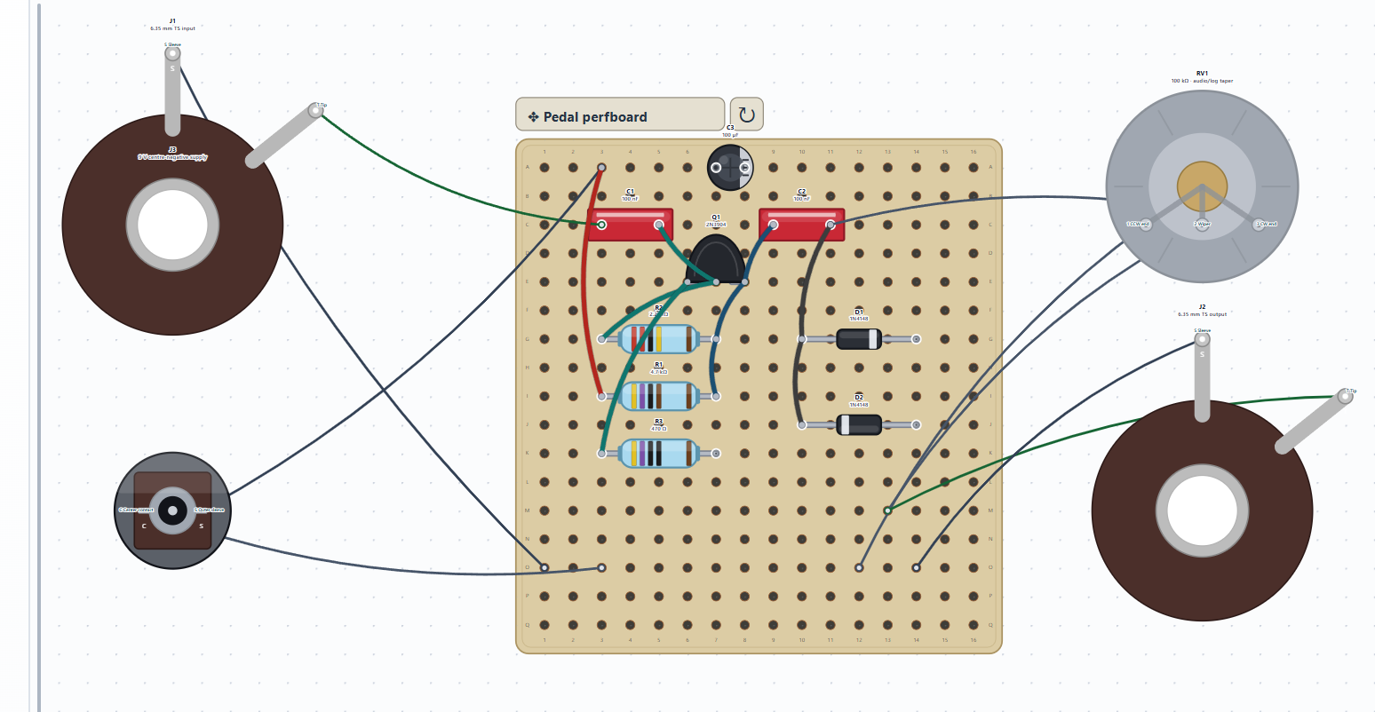
Open Perfboard build and Fit board to window. Use the 16-column × 17-row reviewed layout. Displayed A1 is internal r1c1; displayed G14 is r7c14. Pads start isolated. This guide reproduces the existing checked arrangement, including off-board hardware, rather than proposing an unchecked alternative placement.
11. Place Q1 and both opposed diodes
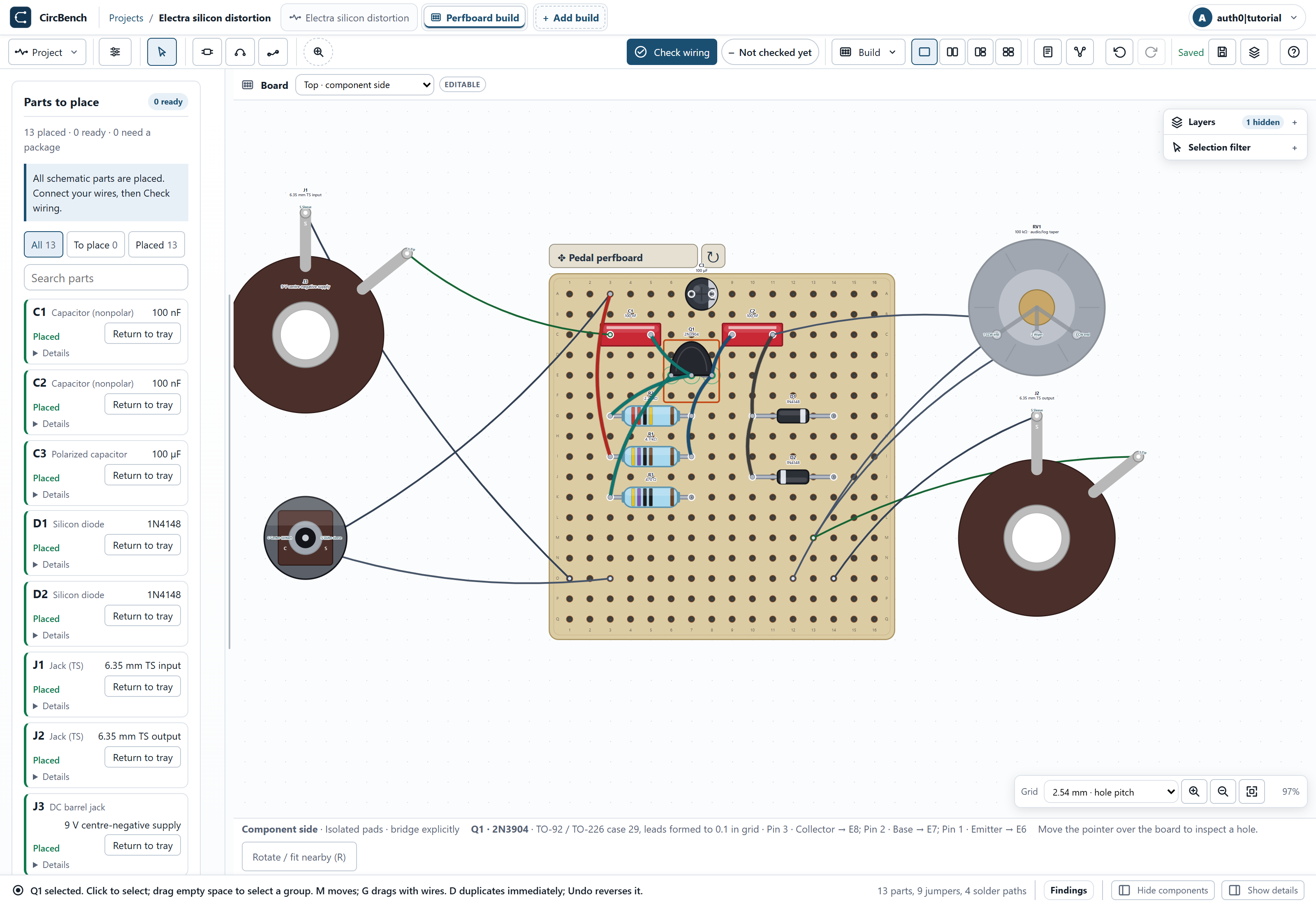
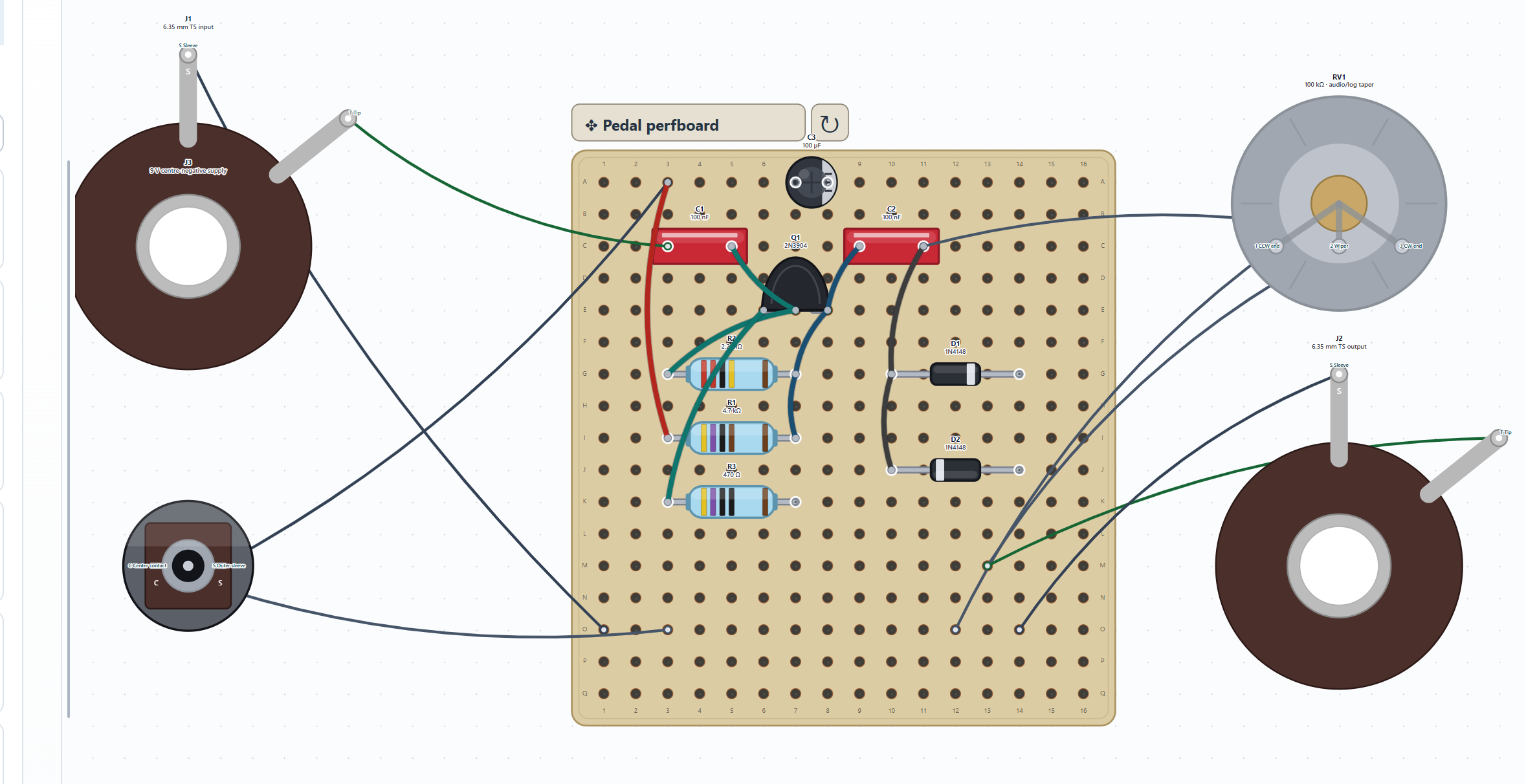
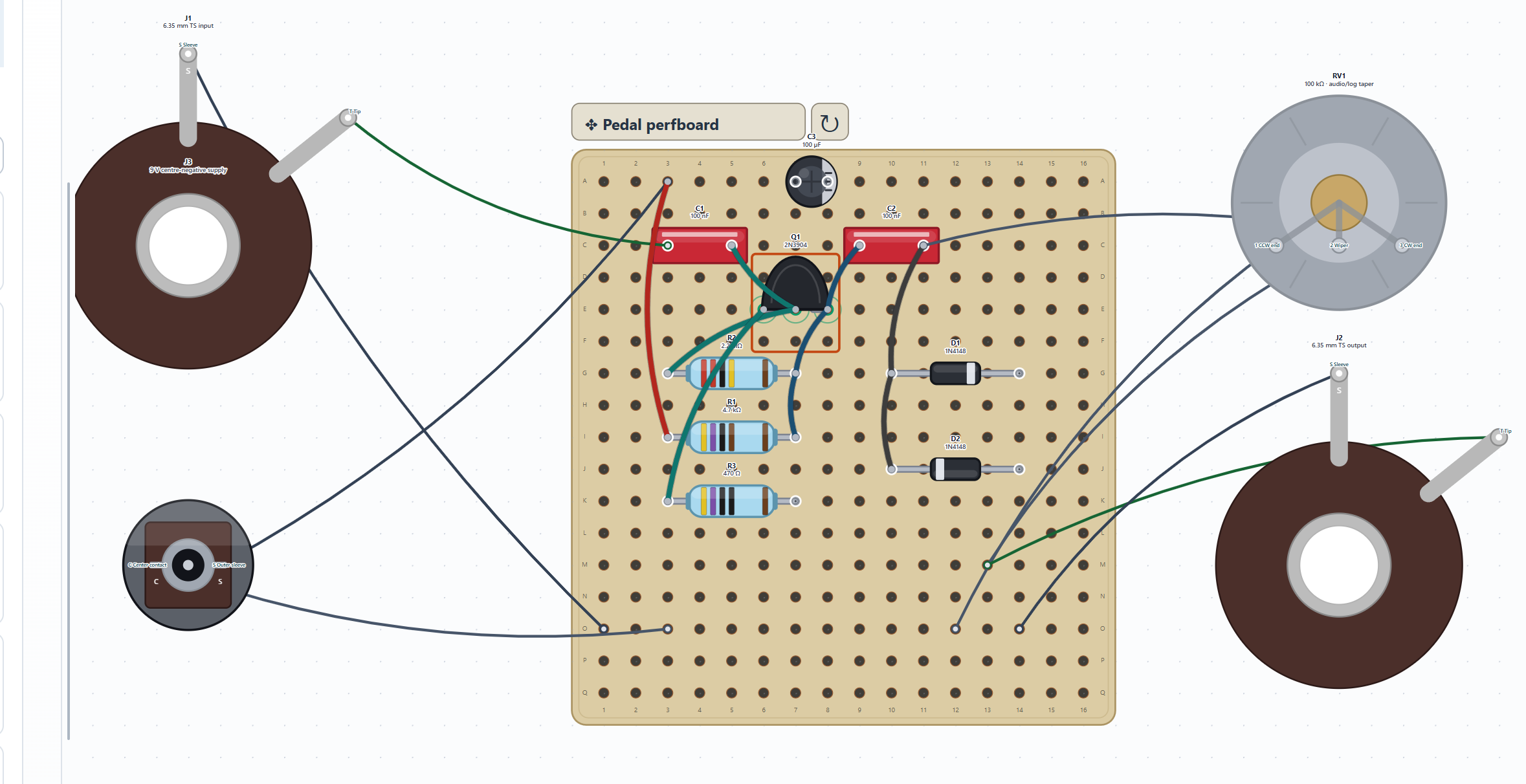
Q1 E/B/C go to E6/E7/E8. C1 spans C3–C5, C2 C9–C11; R1 I3–I7, R2 G3–G7 and R3 K3–K7. D1 A/K go to G10/G14; D2 K/A go to J10/J14. Their opposite cathode directions are intentional. Use the full-size image and attachment schedule to verify each terminal.
12. Reproduce all four solder paths
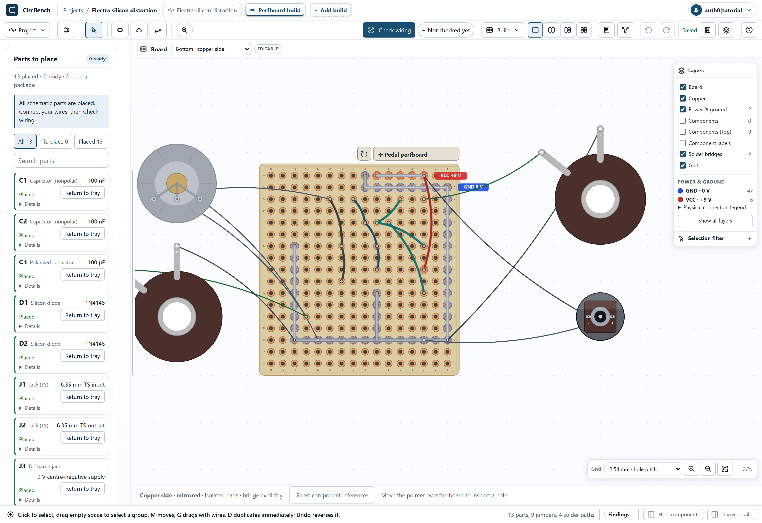
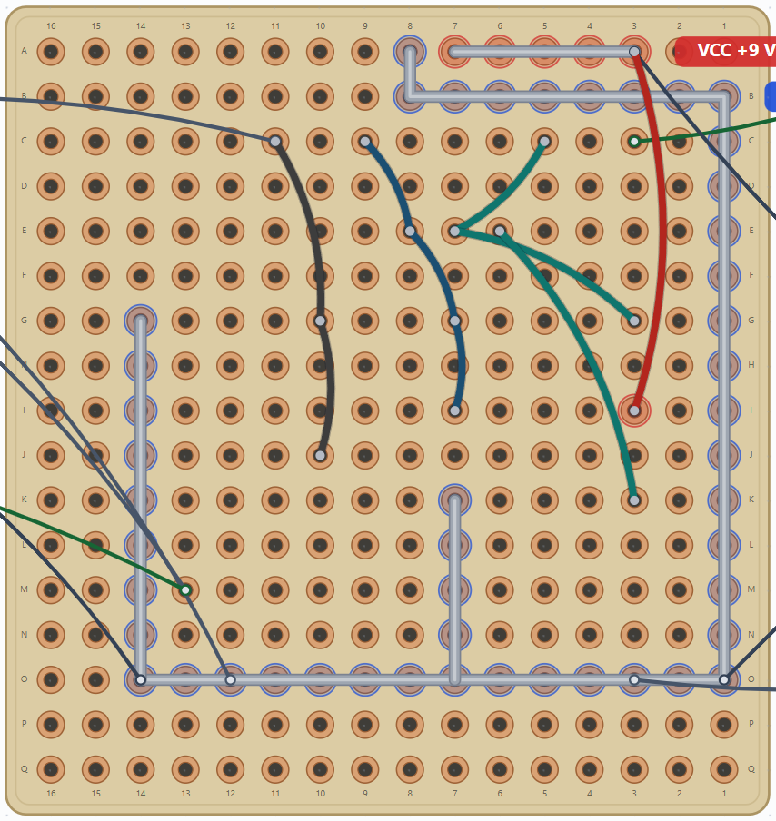
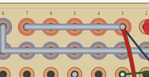
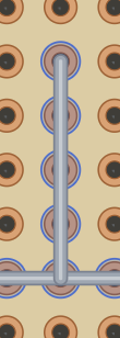
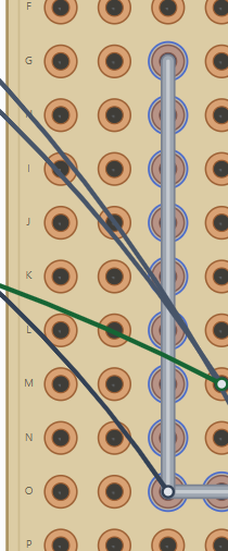
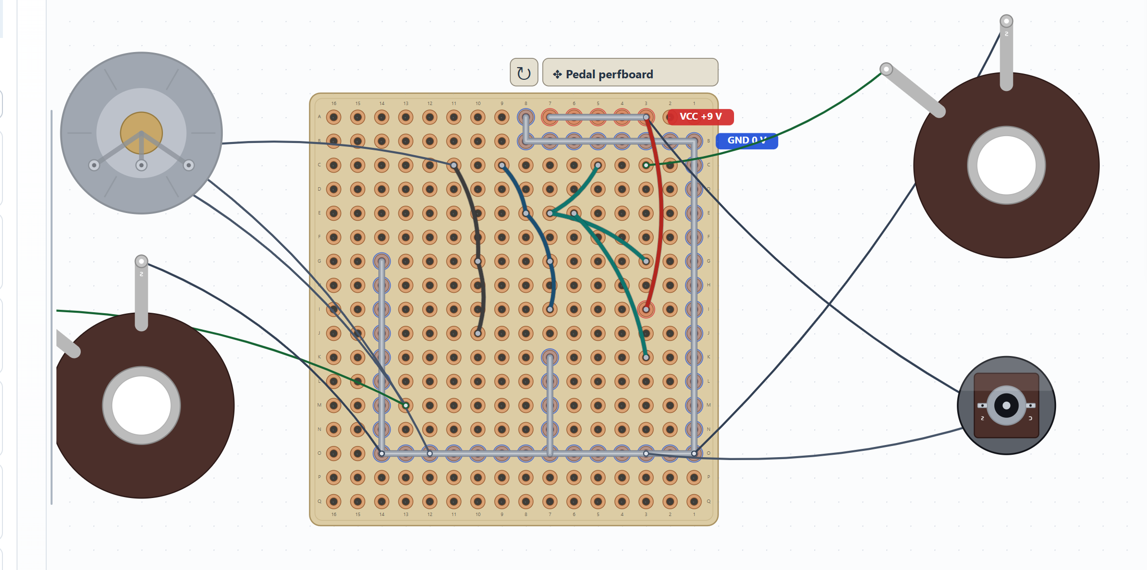
Select the mirrored copper face. The long return path runs from A8 through B8, across B to B1, down column 1 to O1 and across O to O14. Supply uses A3–A7; emitter return uses K7–O7; diode return uses G14–O14. The schedule below expands every intervening contact. These are continuous solder paths, not insulated jumpers.
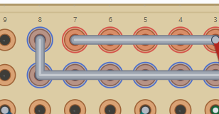

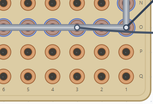
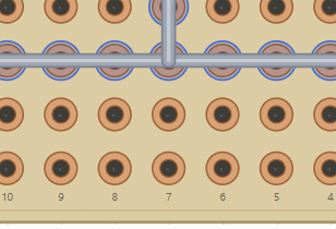
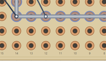
13. Add jumpers and panel hardware
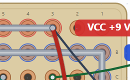
Return to component view. Add the nine board jumpers and mapped jack/pot/DC attachments listed below. Trace C5→E7→G3 as base, C9→E8→G7→I7 as collector, and C11→G10→J10 as clipping signal. E6→K3 joins emitter to its resistor. Keep the clipping return distinct until the authored return path joins it.
Exact reviewed connection schedule
The following tables come from the same versioned backup. Terminal identities belong to the fitted part; letter/number contacts belong to the board. In the copper view the picture mirrors, but these labels retain their identity.
| Part | Logical terminal → board contact |
|---|---|
| J1 | T → C3; S → O1 |
| C1 | 1 → C3; 2 → C5 |
| Q1 | E → E6; B → E7; C → E8 |
| R1 | 1 → I3; 2 → I7 |
| R2 | 1 → G3; 2 → G7 |
| C2 | 1 → C9; 2 → C11 |
| RV1 | 1 → O12; 3 → C11; W → M13 |
| J2 | T → M13; S → O14 |
| J3 | S → A3; C → O3 |
| C3 | + → A7; - → A8 |
| R3 | 1 → K3; 2 → K7 |
| D1 | A → G10; K → G14 |
| D2 | A → J14; K → J10 |
| Insulated connection | Endpoint A | Endpoint B |
|---|---|---|
| 1 | C5 | E7 |
| 2 | E7 | G3 |
| 3 | C9 | E8 |
| 4 | E8 | G7 |
| 5 | G7 | I7 |
| 6 | A3 | I3 |
| 7 | C11 | G10 |
| 8 | G10 | J10 |
| 9 | E6 | K3 |
| Solder path | Contacts in order |
|---|---|
| 1 | A8 → B8 → B7 → B6 → B5 → B4 → B3 → B2 → B1 → C1 → D1 → E1 → F1 → G1 → H1 → I1 → J1 → K1 → L1 → M1 → N1 → O1 → O2 → O3 → O4 → O5 → O6 → O7 → O8 → O9 → O10 → O11 → O12 → O13 → O14 |
| 2 | A3 → A4 → A5 → A6 → A7 |
| 3 | K7 → L7 → M7 → N7 → O7 |
| 4 | G14 → H14 → I14 → J14 → K14 → L14 → M14 → N14 → O14 |
Check, repair and preserve the project
14. Run a fresh independent wiring check
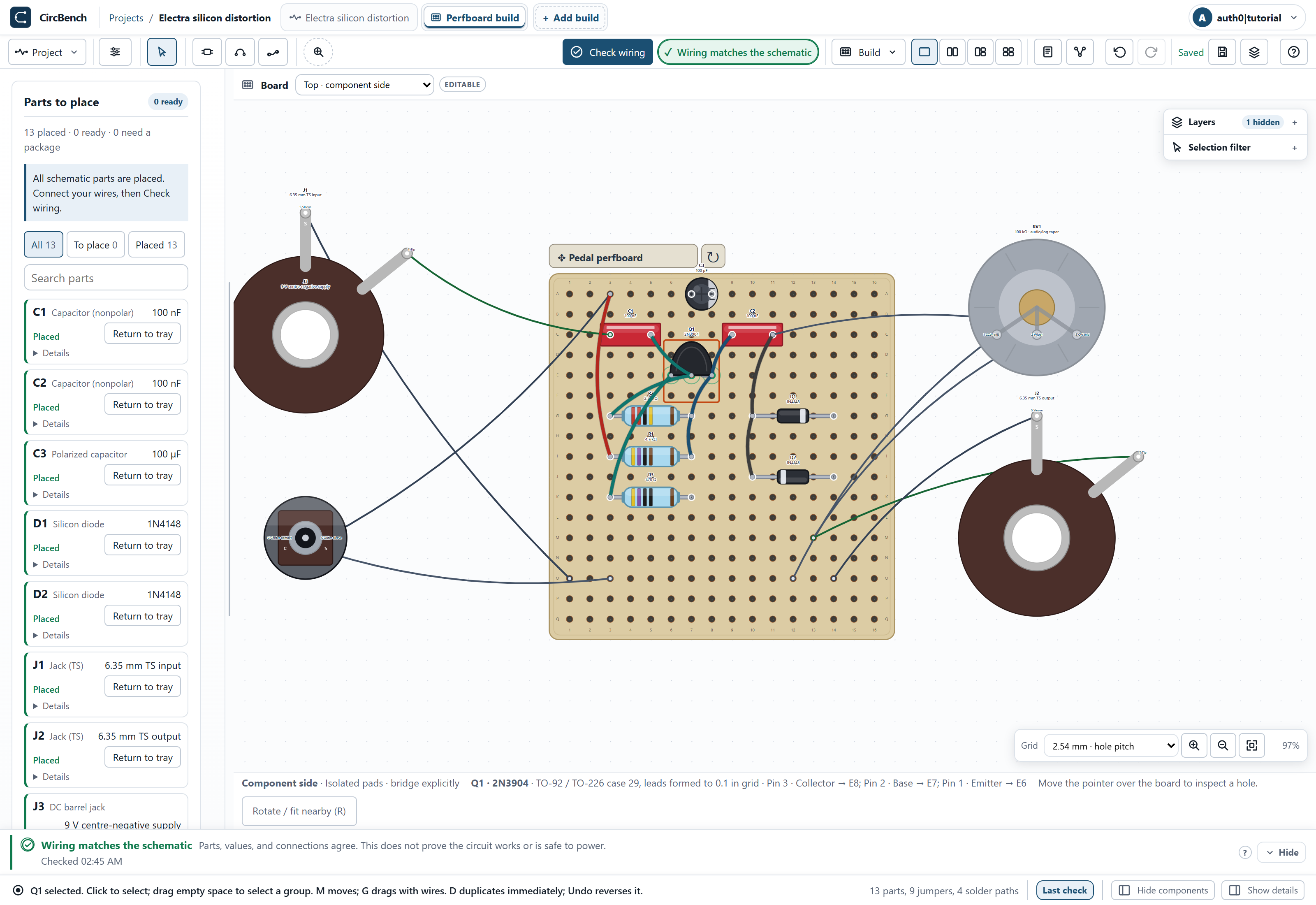
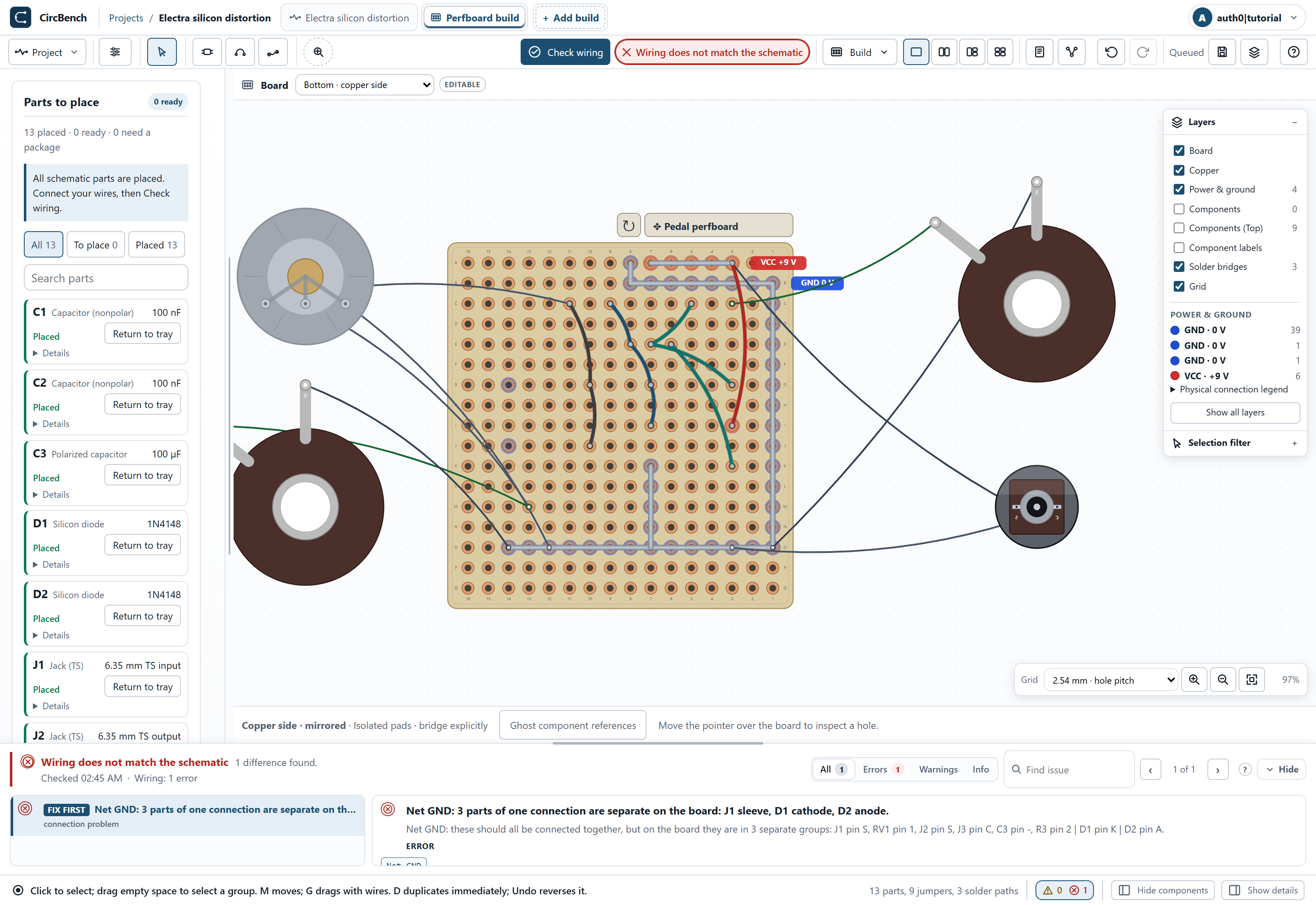
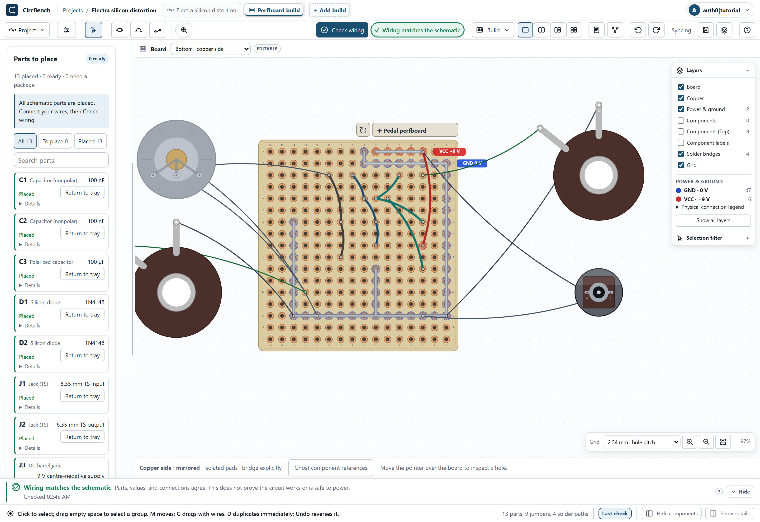
Choose Check wiring and wait for the completed match. CircBench extracts the represented board connections independently and compares them with the schematic. If your copy differs, reveal each reported open or short, verify both endpoints and check unplaced parts or fitted mappings. A previous or pending result is not a fresh match.

15. Introduce a deliberate wiring fault
On the copper face, delete the G14–O14 clipping-return solder path and run a new Check wiring. The physical clipping network now has an open while the schematic is unchanged. This is the exact fault fixture used for the guide. A diode flip is a different experiment and is not claimed to always cause a connectivity mismatch.

16. Undo the fault and prove the repair
Choose Undo to restore the deleted connection or cut. Run Check wiring again and wait for a fresh match. Undo alone is not verification: the completed check proves the represented topology was restored. Keep this repaired version for the following persistence and download checks.

17. Save, reload and check again
Wait for the normal save indicator, then reload the page. Open the same build and run Check wiring again. Confirm a fresh match after reload. If saving reports a problem, open save recovery and export a backup; do not assume remote account storage succeeded merely because the editor still displays the project.
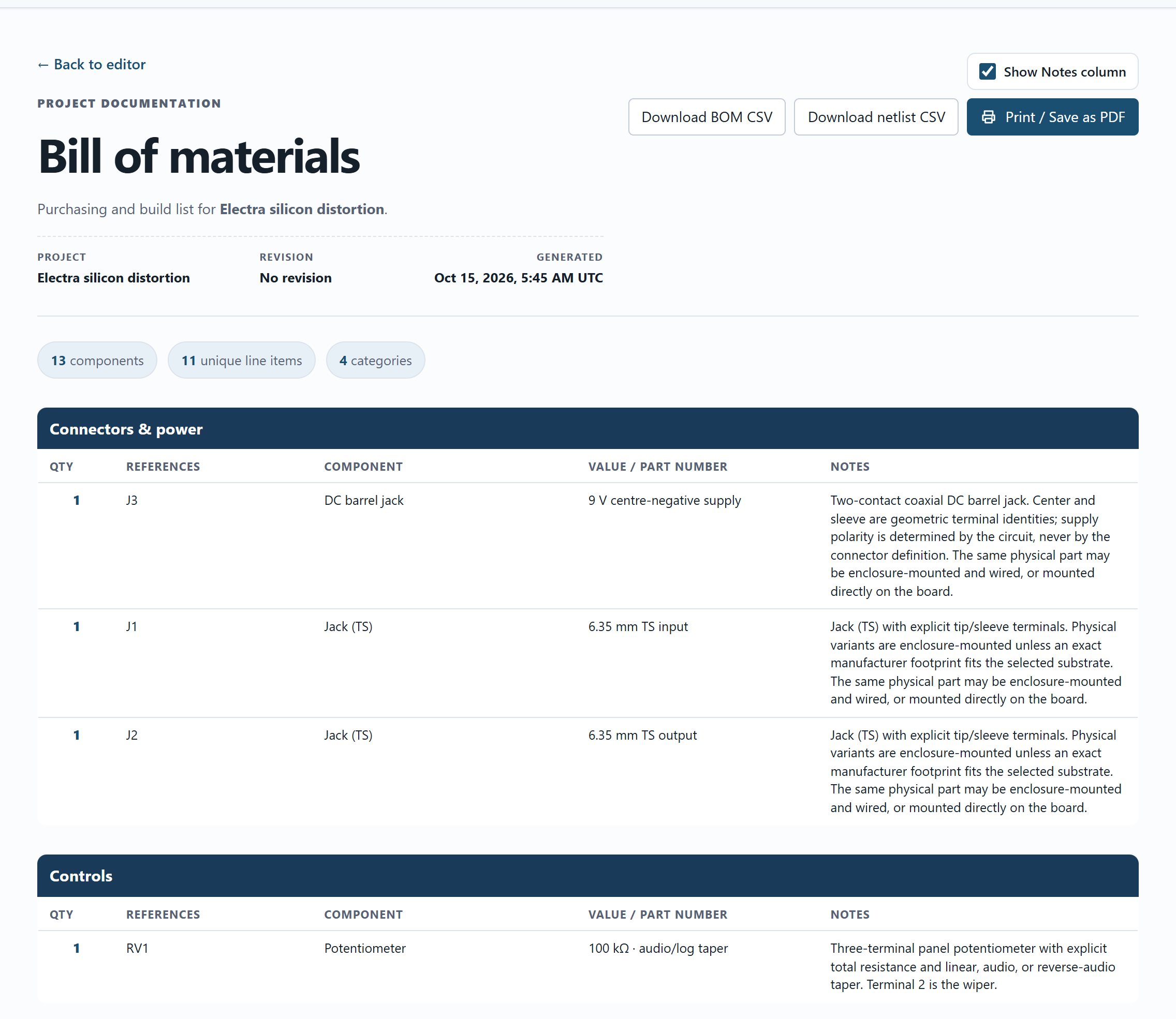
18. Inspect and export the parts list
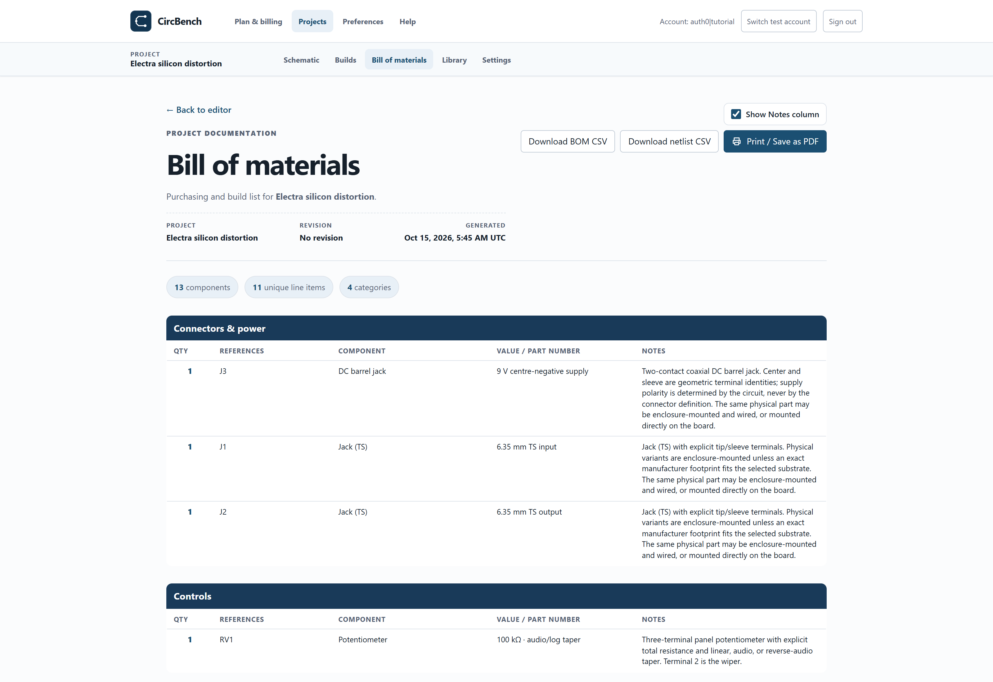
Open Bill of materials, review the fitted parts, values and quantities, then use Export CSV. Compare it with the versioned parts list above. A BOM lists represented parts; it does not select manufacturer voltage ratings or prove that a purchased package has the same terminal order. Resolve substitutions before physical assembly.
19. Export a portable project backup
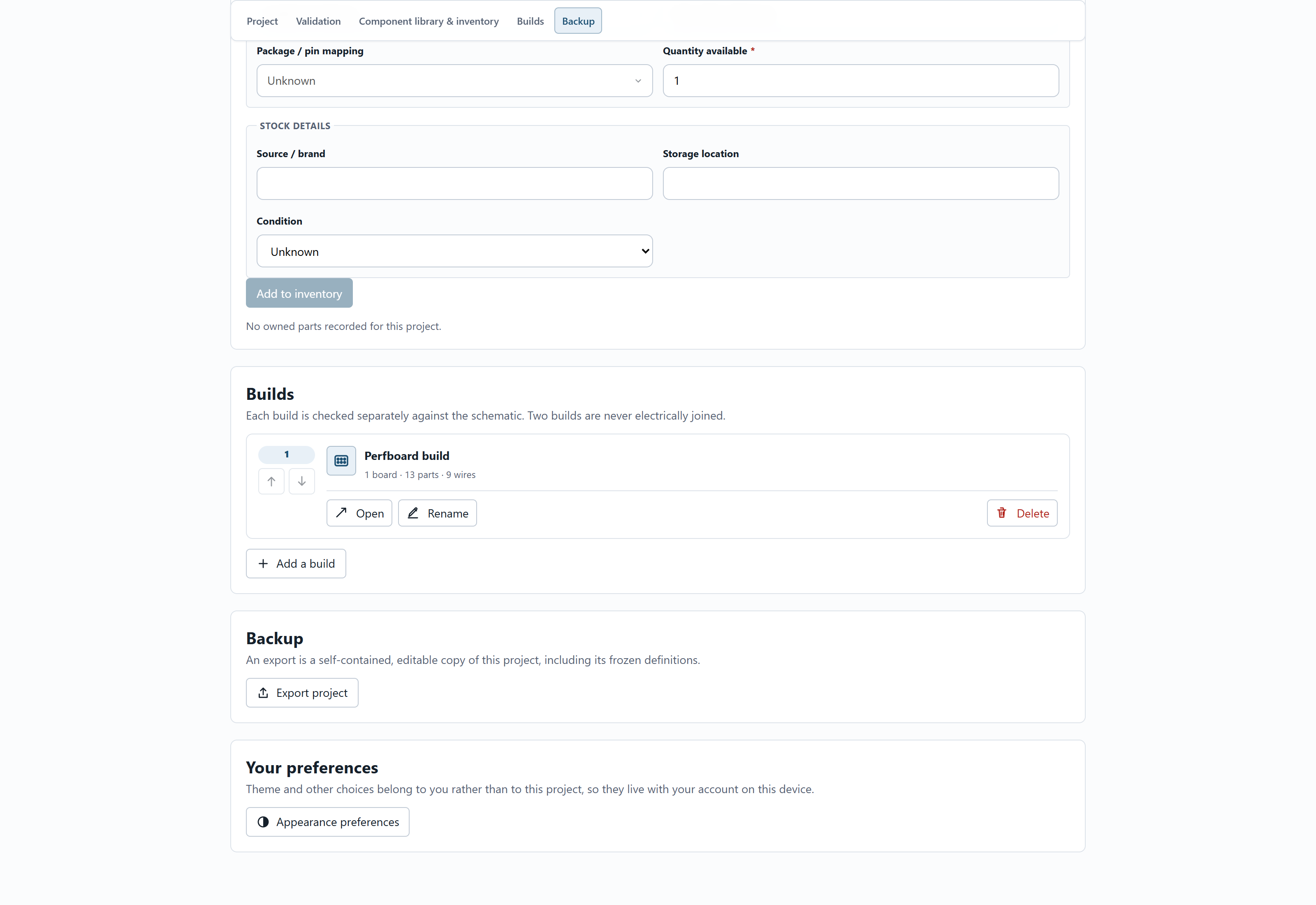
Open project Settings, go to backup and choose Export project. Keep the resulting .circbench.json file. This preserves the schematic, fitted build, definitions and saved bench/model settings. Raw simulation vectors and uploaded audio are separate outputs and are not retained in this project backup.

20. Import the backup and recheck
Return to Projects and Import the backup file. The imported copy appears in your library; explicitly Open its schematic, then its build. Run Check wiring and confirm a new match. If an import is rejected, keep the original file and compare its schema/version with the app rather than editing integrity fields by hand.
What this result establishes
The modeled result is not a physical clipping measurement. This variant does not qualify a historical unit, device spread, noise, maximum ratings, enclosure, power protection or footswitch wiring. A connectivity match cannot establish those properties.
The screenshots show current solver results and fresh wiring checks for this exact example version. They do not assert that hardware was assembled, measured or qualified. Use the supplied source, load and stimulus settings when comparing results.
Circuit credit: Jack Orman’s documented Electra circuit and variants. CircBench authors its own drawing, independent perfboard layout, 100 kΩ audio level control, 100 µF supply filter and explicit nominal testbench.
Your next project
Compare headroom with the single-transistor boost and nonlinear bias interaction with the stripboard fuzz.