perfboard · beginner
Build and simulate a passive treble-cut circuit
Draw an RC guitar treble cut, understand its loaded response, and reproduce a checked perfboard build with clear screenshots and project downloads.
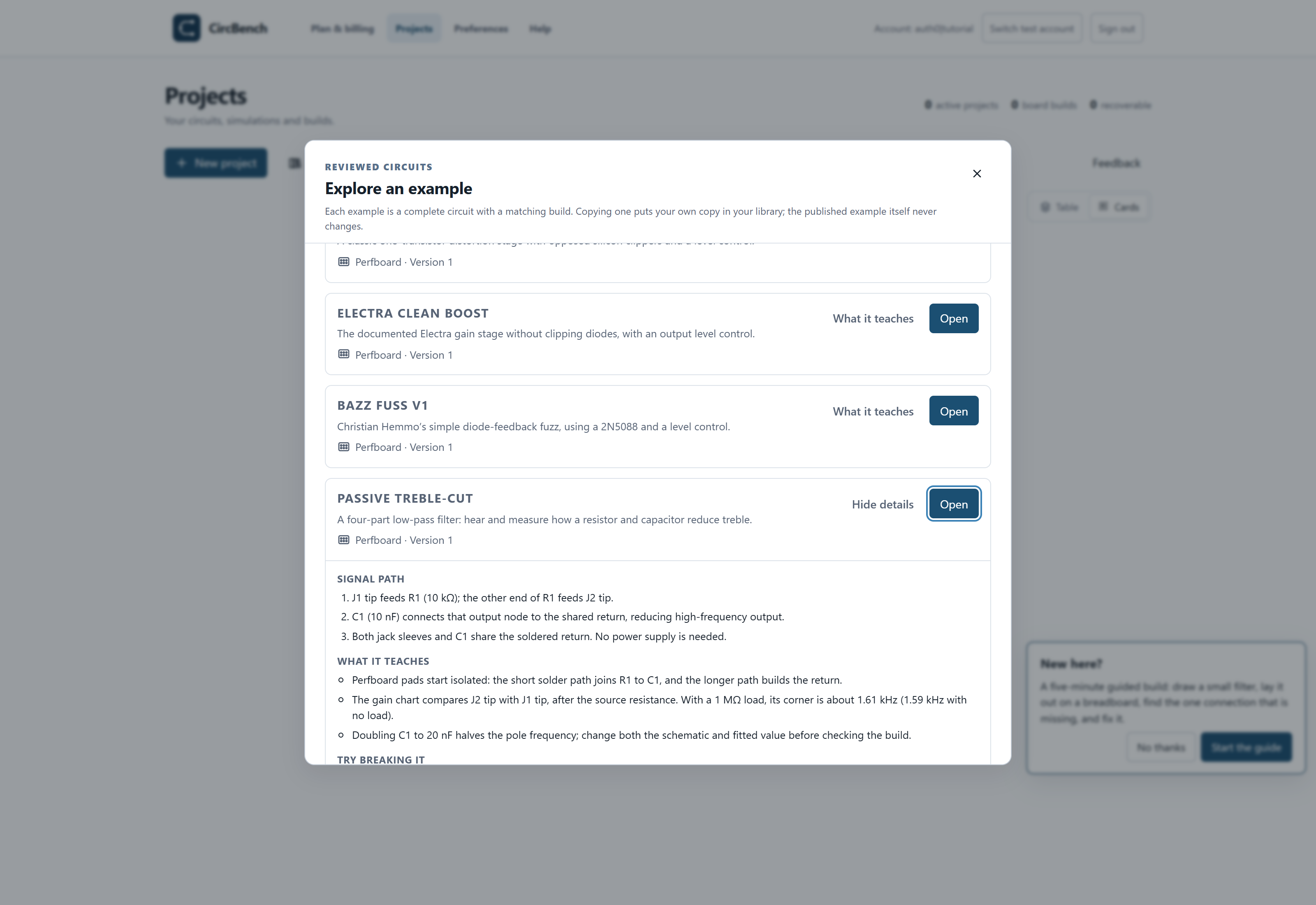
The app opens the current example chooser. Choose Open to create your own account copy. For this guide's exact v1, download and import the project backup if the catalog version has changed.
A resistor and capacitor are enough to make a useful lesson in guitar treble loss. This fixed-value circuit passes low frequencies more readily than high ones. You will trace its schematic, compare two capacitances, and inspect every explicit connection on an 8 × 6 perfboard. It has no battery and passes DC; it is not a complete adjustable guitar tone control.
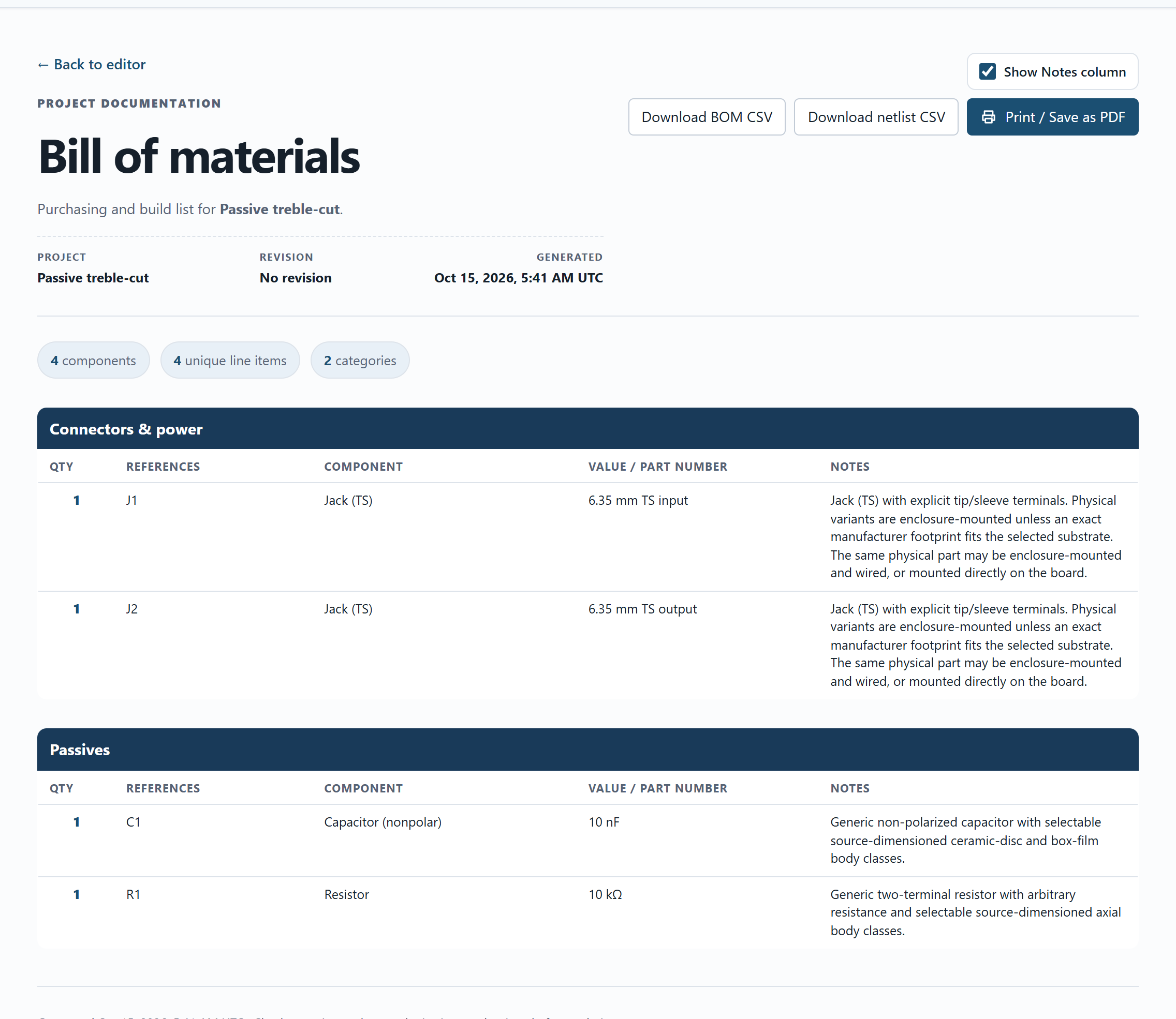
Parts: R1 10 kΩ; C1 10 nF; two 6.35 mm TS jacks. Use the downloadable BOM for the fitted package and terminal mappings.
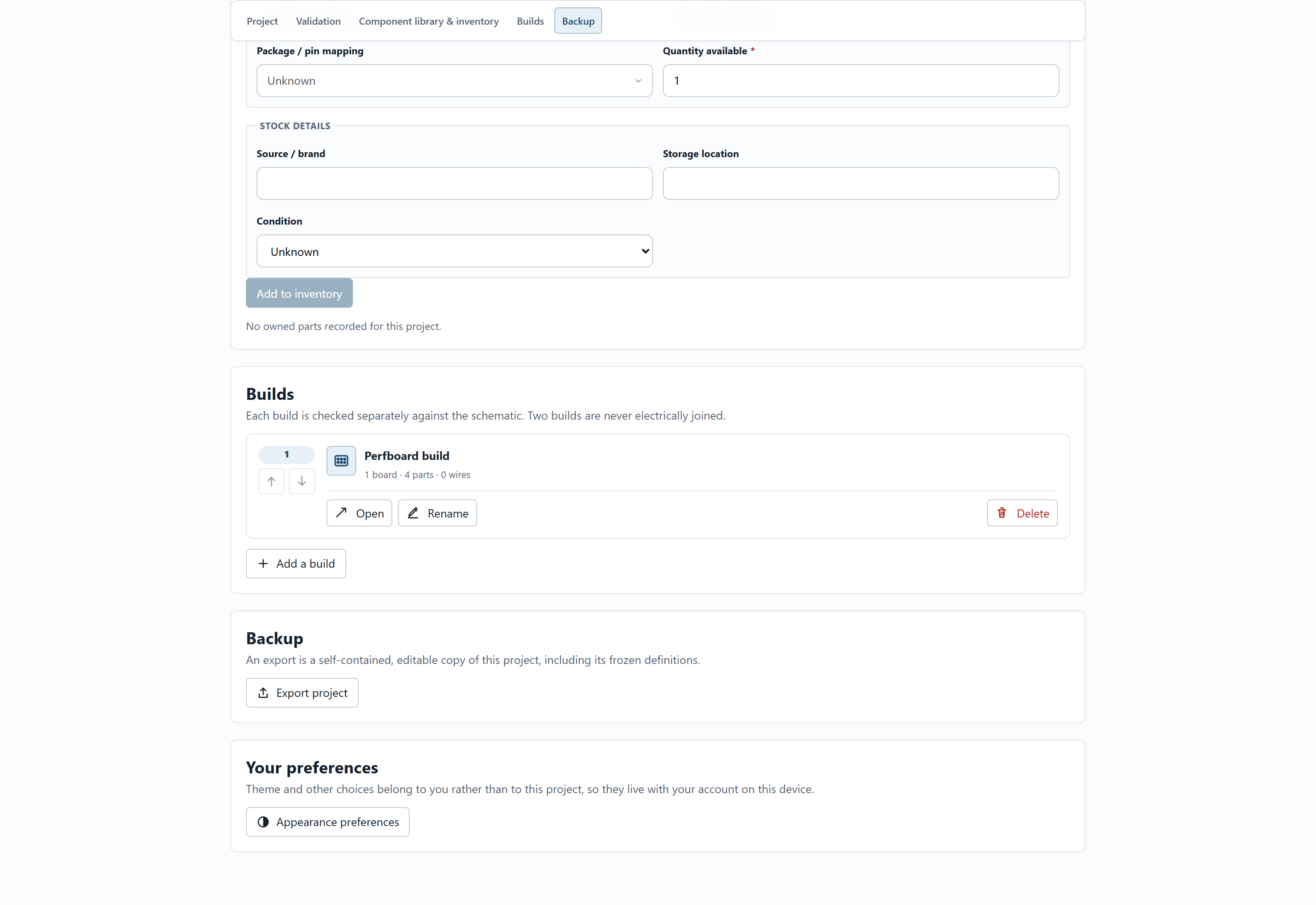
Before starting: have a CircBench account and use a copy for experiments. This is a software build and simulation walkthrough; the images are actual application screenshots, not photographs of assembled hardware. Every numbered step has a detail image and a link to its unmodified full context PNG. Open full size when comparing small pin labels, especially on a phone.
Draw and understand the schematic
1. Open the exact reviewed example
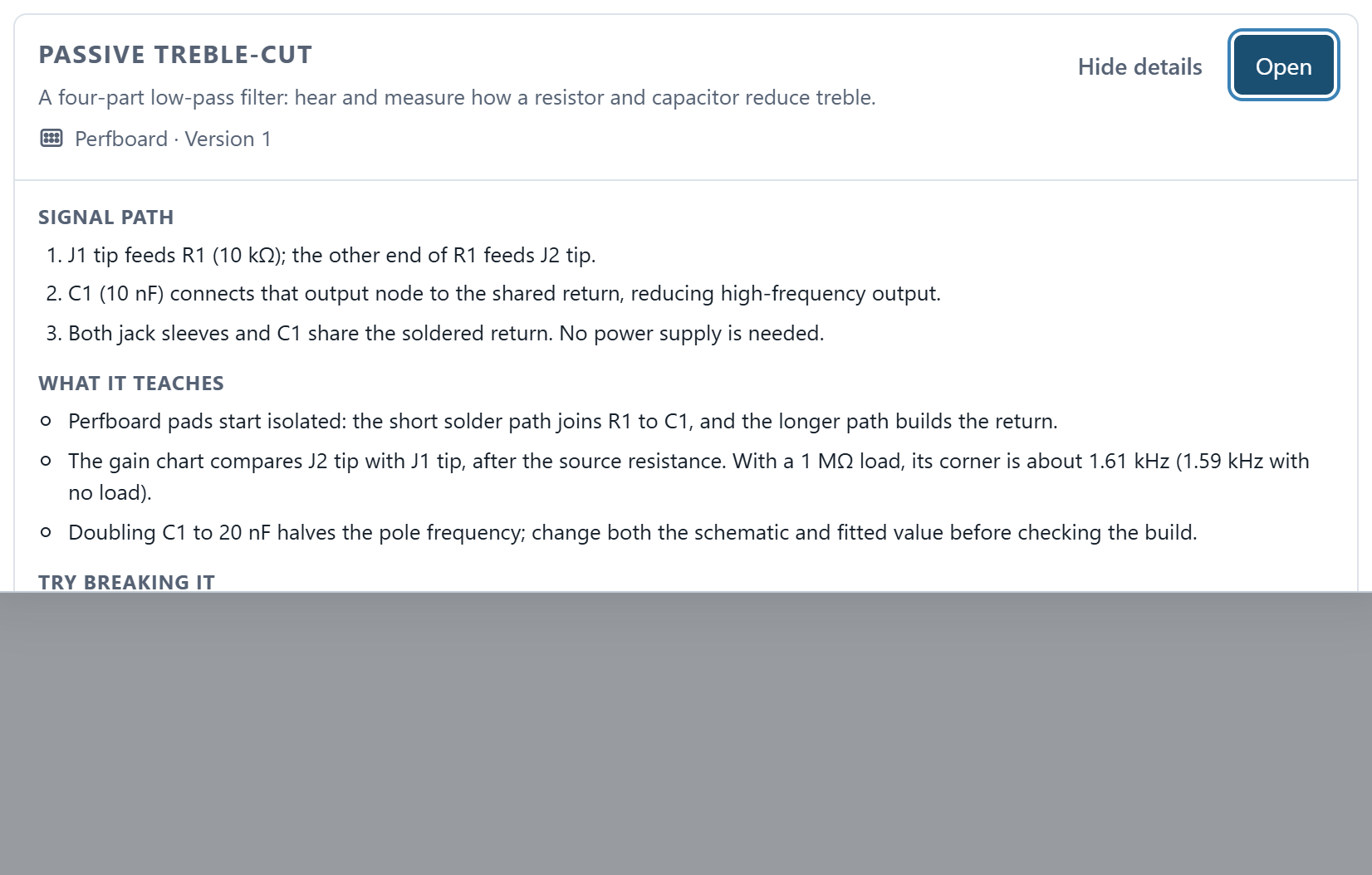
Use the example link above, sign in if requested, and confirm Passive treble-cut, version 1 in Explore an example. Choose Open to create your own account copy. The link alone does not create a project. If the catalog changes, import the versioned backup above to follow this precise guide. All screenshots show the actual reviewed copy, with completed wiring as a reference for your own drawing.
2. Inspect the series resistor
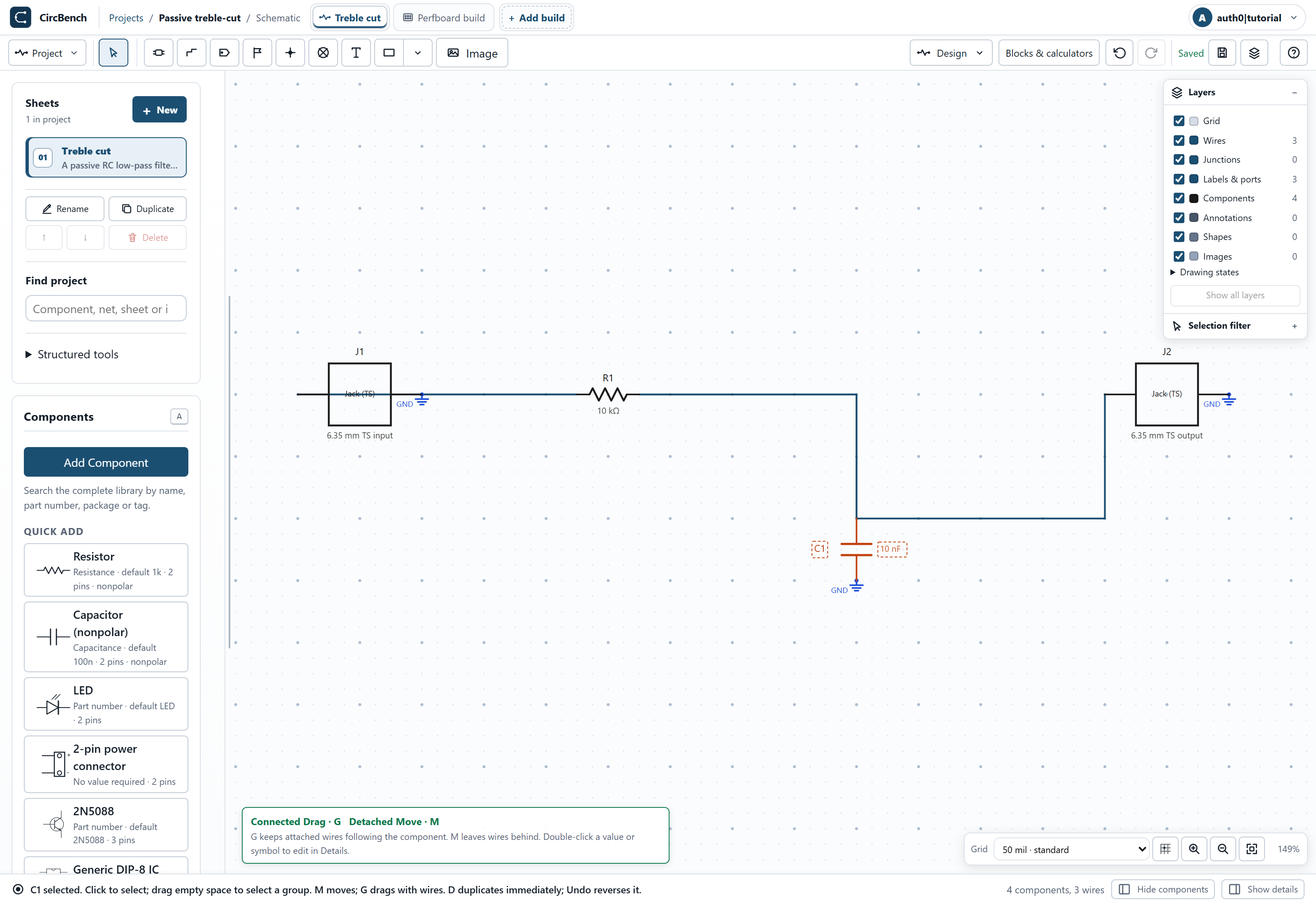
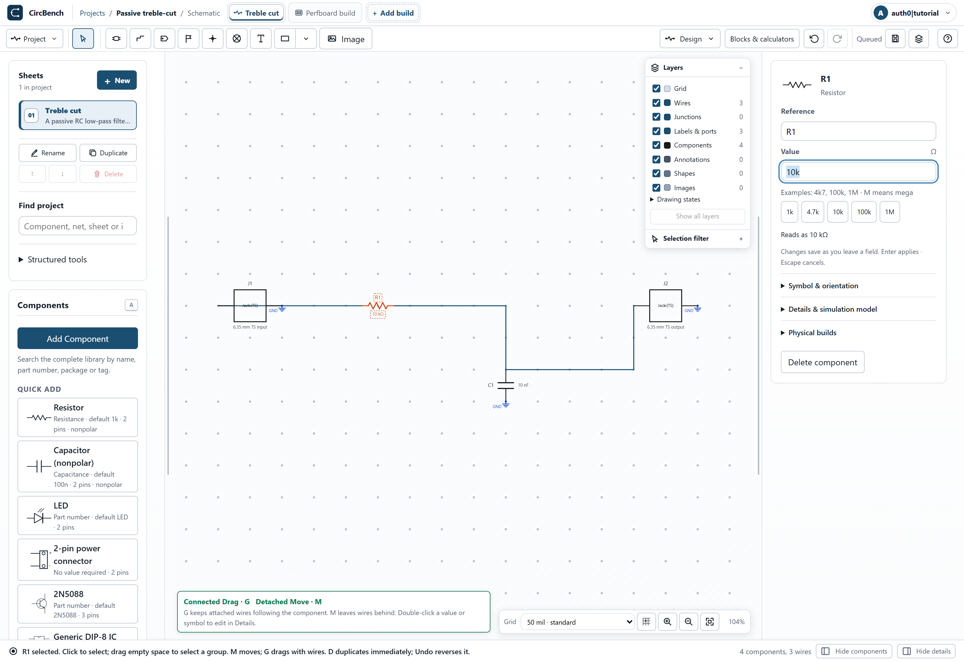
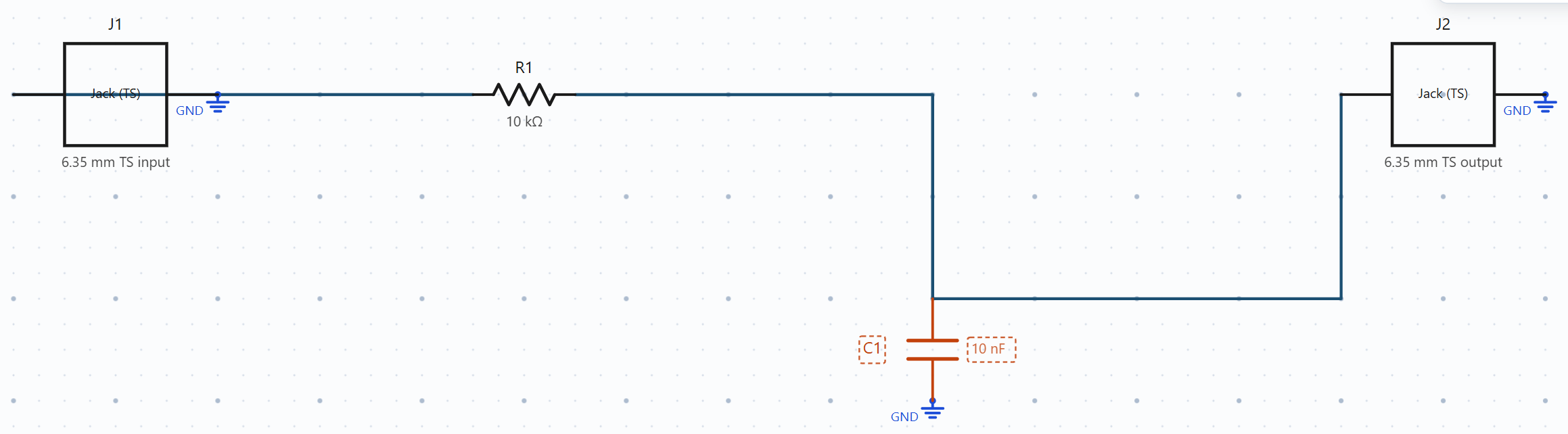
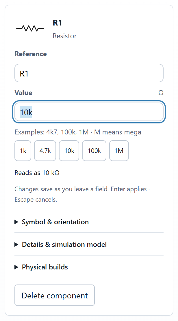
In Schematic, double-click R1 to open Details. Confirm 10 kΩ. To redraw the circuit, place a resistor and set its Value to 10k; place input and output TS jack symbols on either side. R1 belongs between the two tips, not between a tip and sleeve. The screenshot inspects the completed reference copy.
3. Add the shunt capacitor
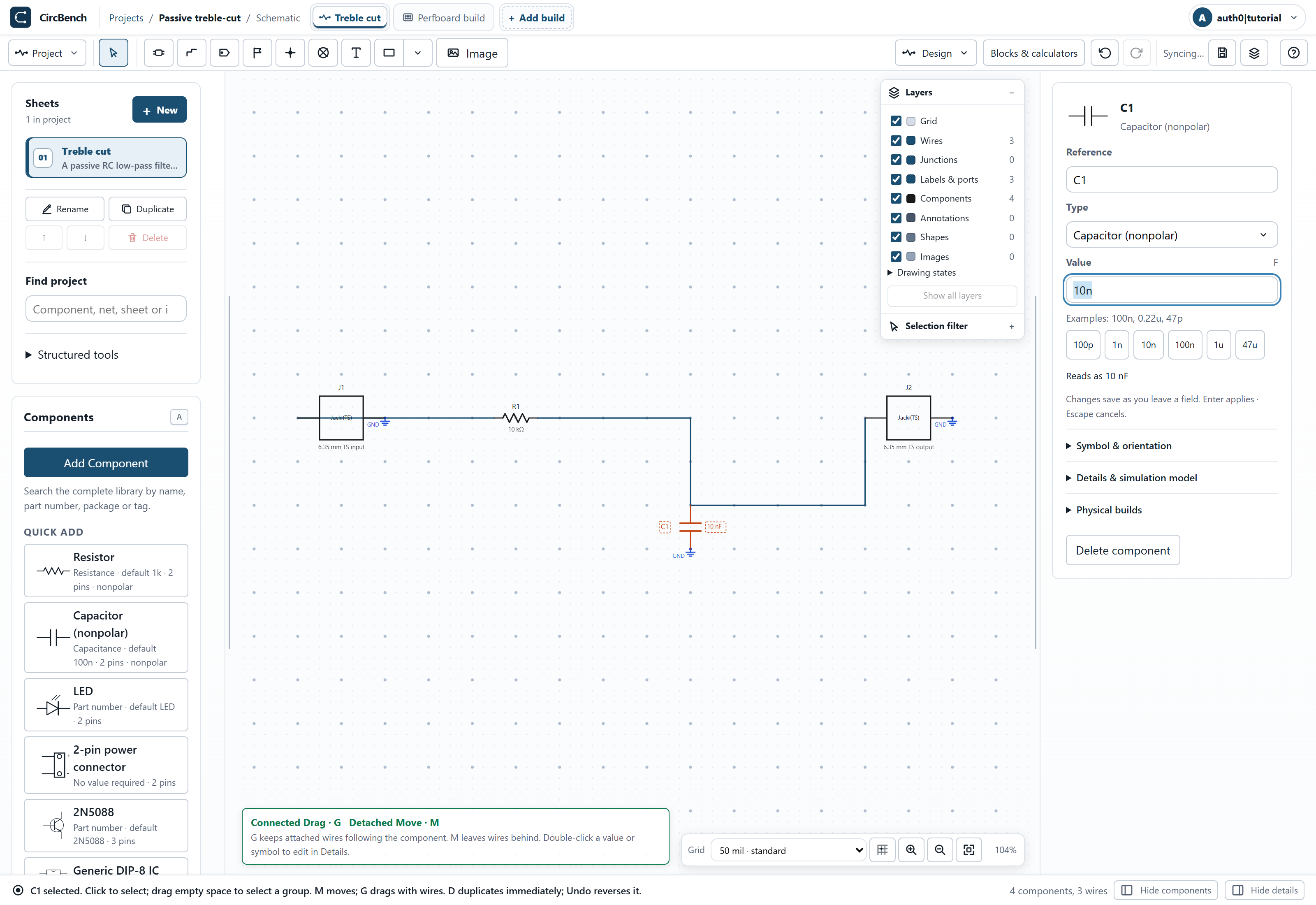
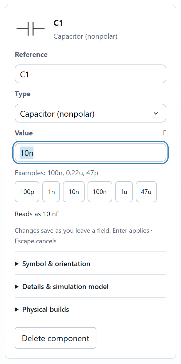
Inspect C1 and confirm 10n (10 nF). When drawing your own copy, connect one C1 terminal to the output end of R1, then its other terminal to common return. This film capacitor is nonpolar. Its falling impedance with frequency diverts more high-frequency signal away from the output.
4. Trace the complete schematic
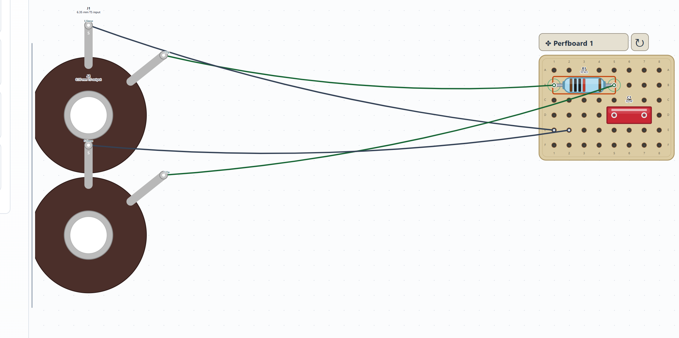
Fit schematic to window. Follow J1 tip → R1 → J2 tip, with C1 from J2 tip to return. Join both jack sleeves to that same return. Start and finish wires on the actual pins; crossings alone do not create a connection. The full-size image lets you compare each wire with the finished reference.
Configure and interpret the simulation
5. Set an explicit passive testbench
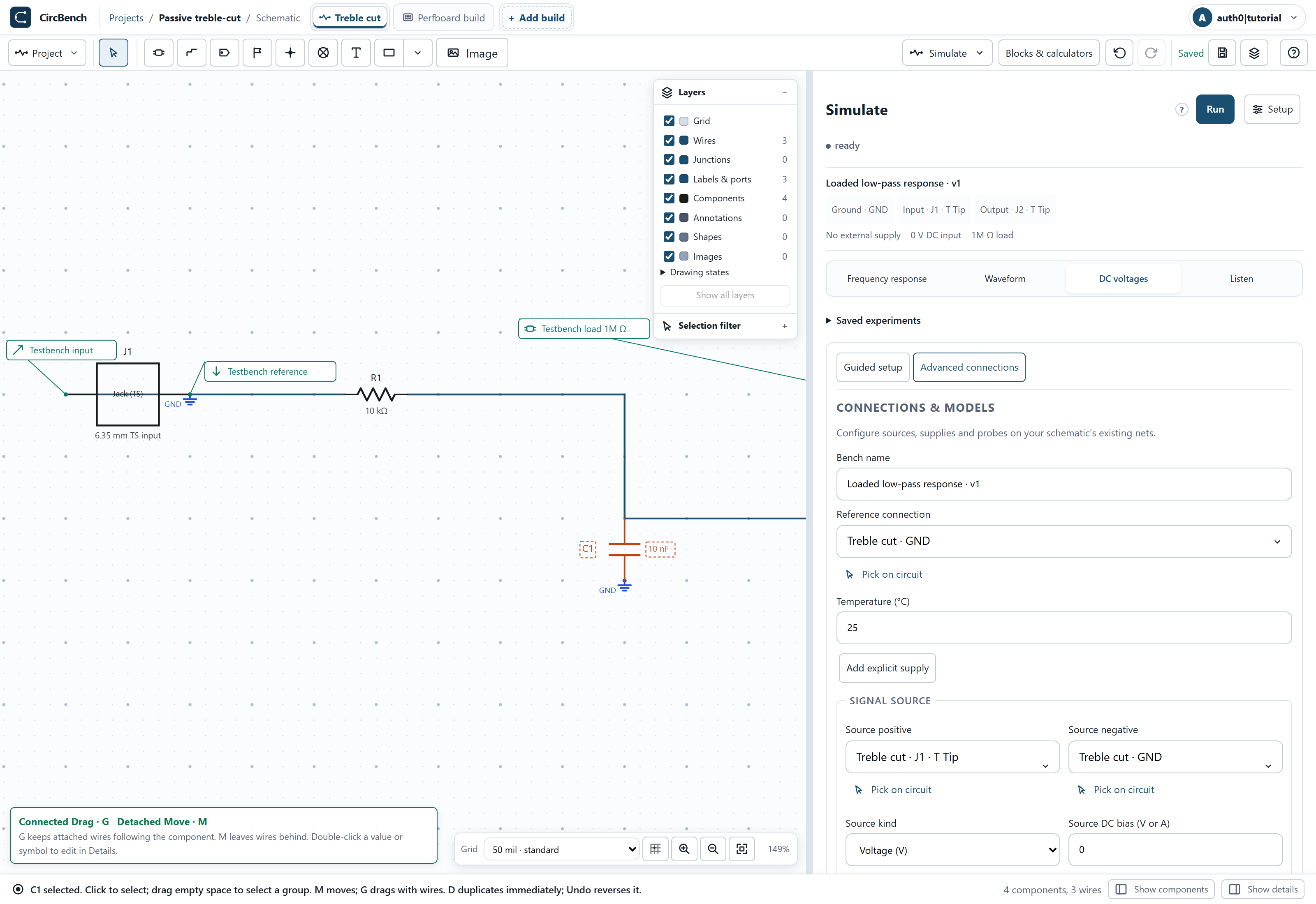
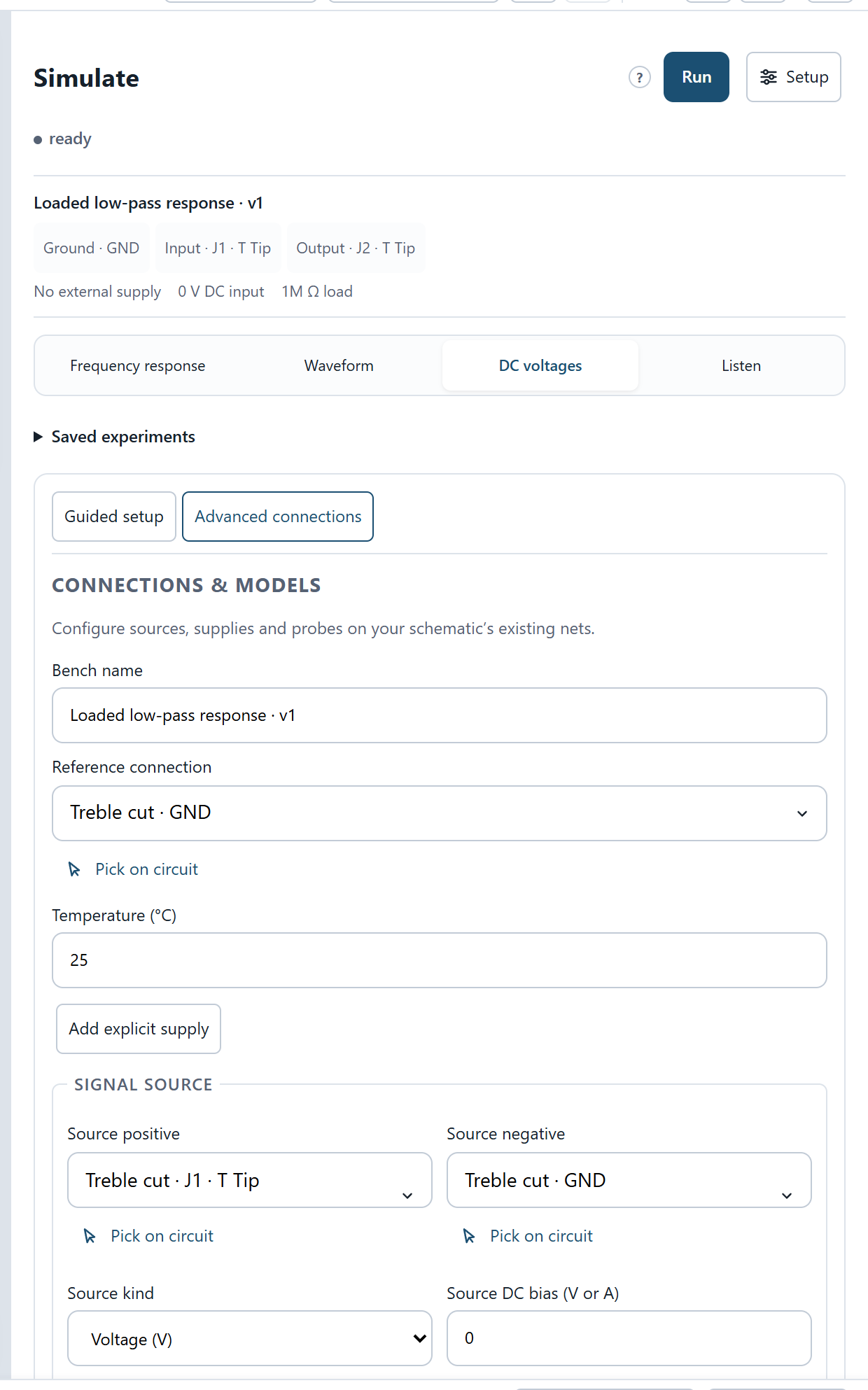
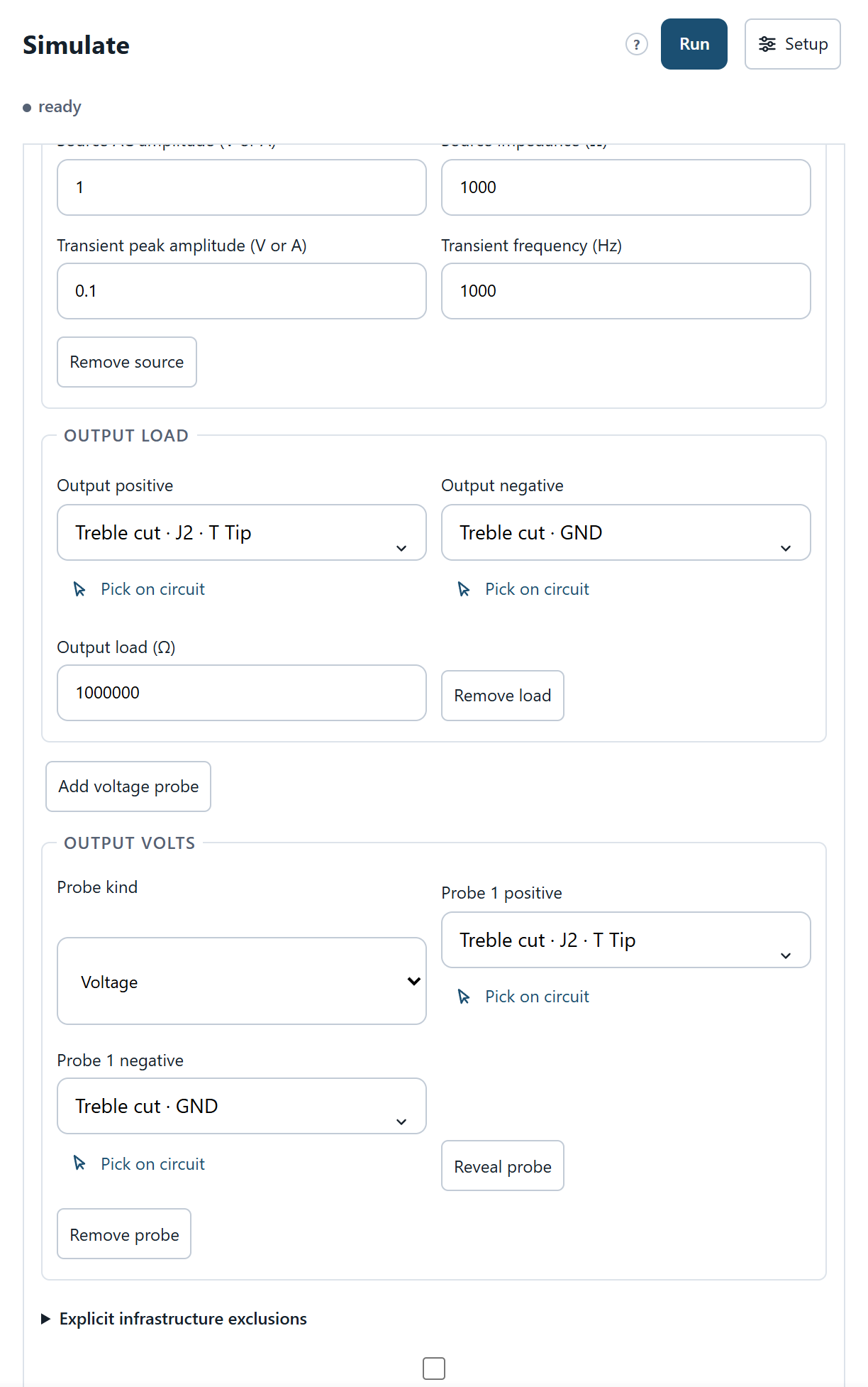
Choose Simulate, then Setup. Reference is GND, input is J1 tip and output/load positive is J2 tip; source and load negative go to GND. Keep 1 kΩ source impedance, 1 MΩ load, 100 mV peak at 1 kHz, and 25 °C. No external supply or active-device model is needed. Save setup.
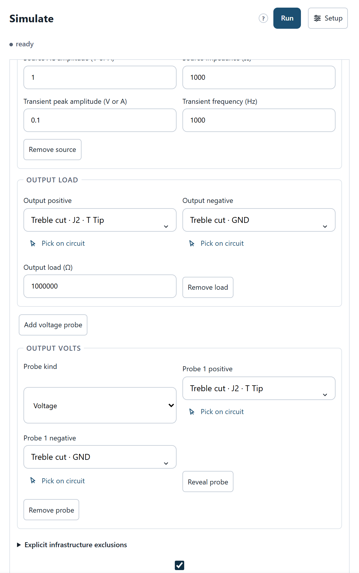
6. Check the zero-signal operating point
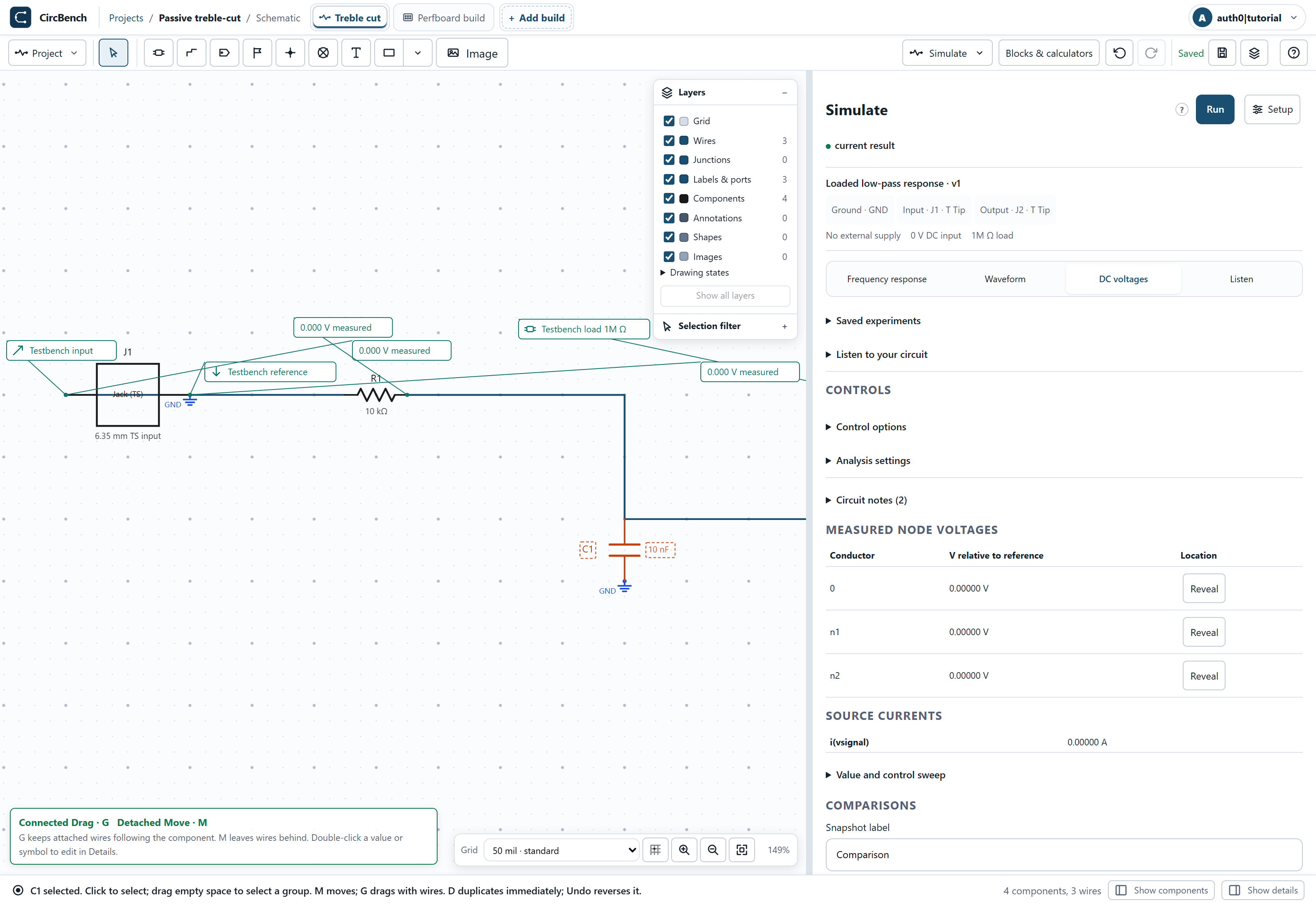
Open Analysis settings, choose DC operating point and Run analysis. Wait for current result. With zero DC input, the signal nodes settle at approximately zero volts. This establishes the reference; it is not the filter response. If results are unavailable, return to Setup and verify the ground and both source terminals.
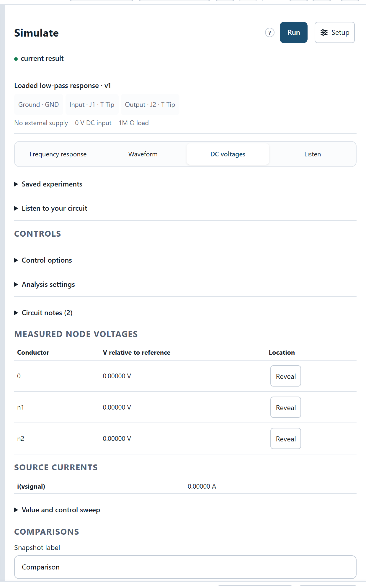
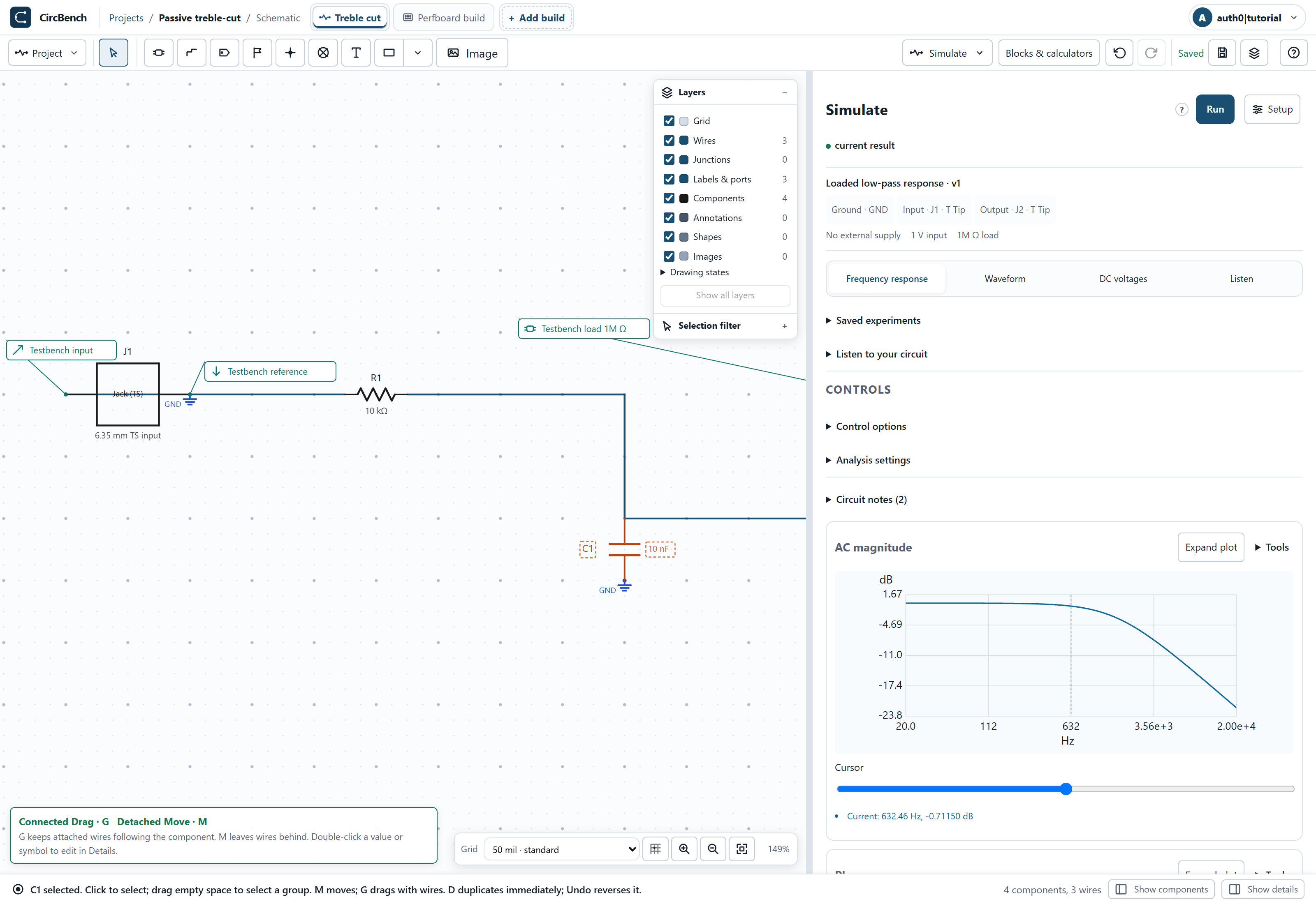
7. Read the frequency response
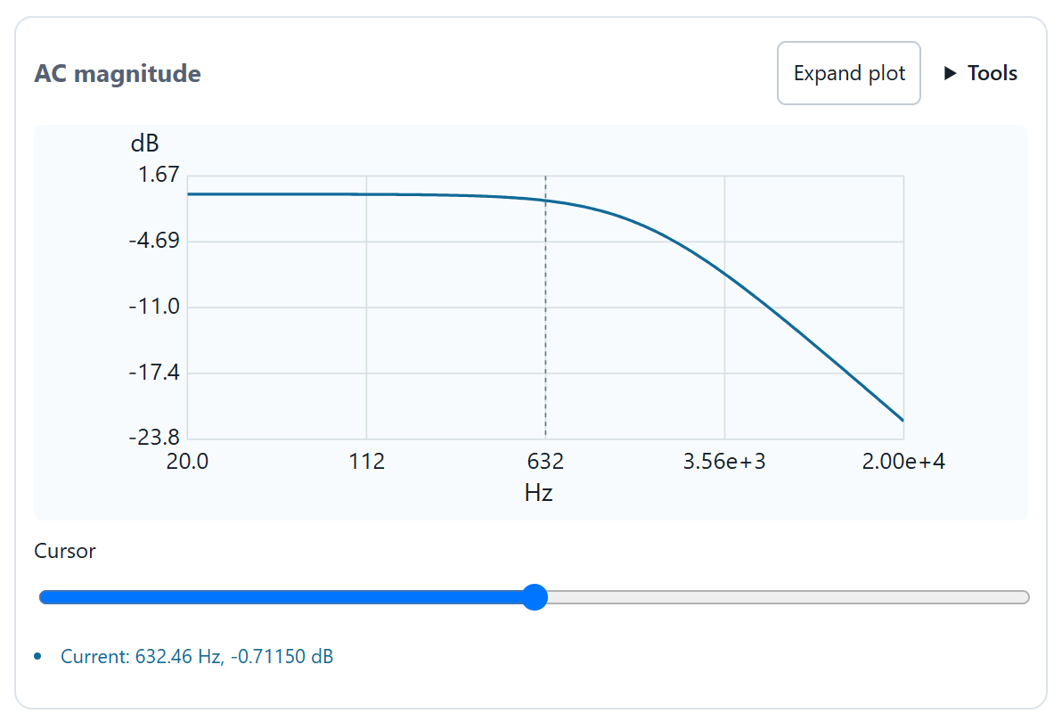
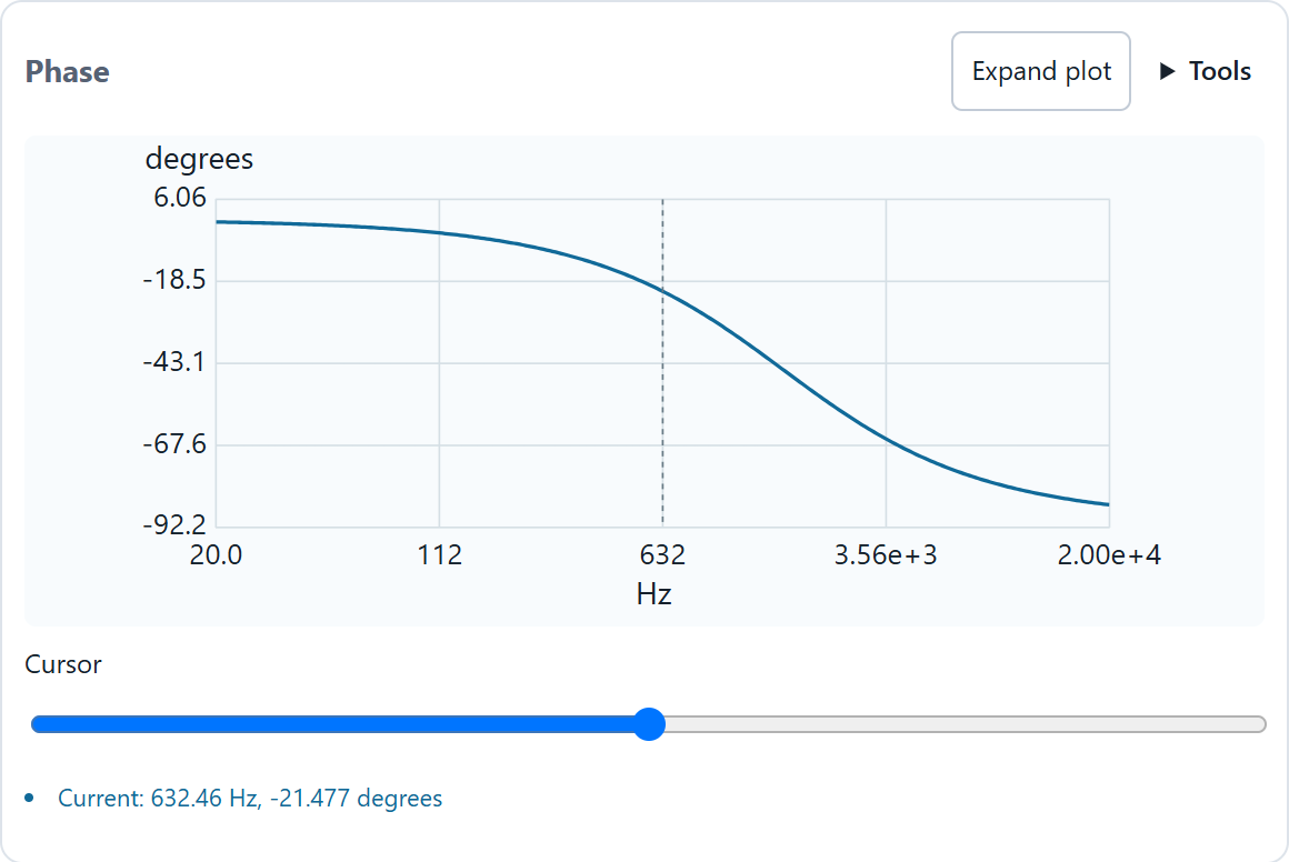
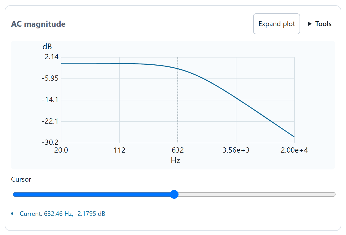
Select AC frequency response and run a fresh analysis from 20 Hz to 20 kHz. Read the magnitude and phase plots separately. The chart compares actual J2 voltage with J1 voltage after the source resistor. The unloaded estimate 1/(2πRC) is 1.59 kHz; with the 1 MΩ output load the J2/J1 pole is about 1.61 kHz.
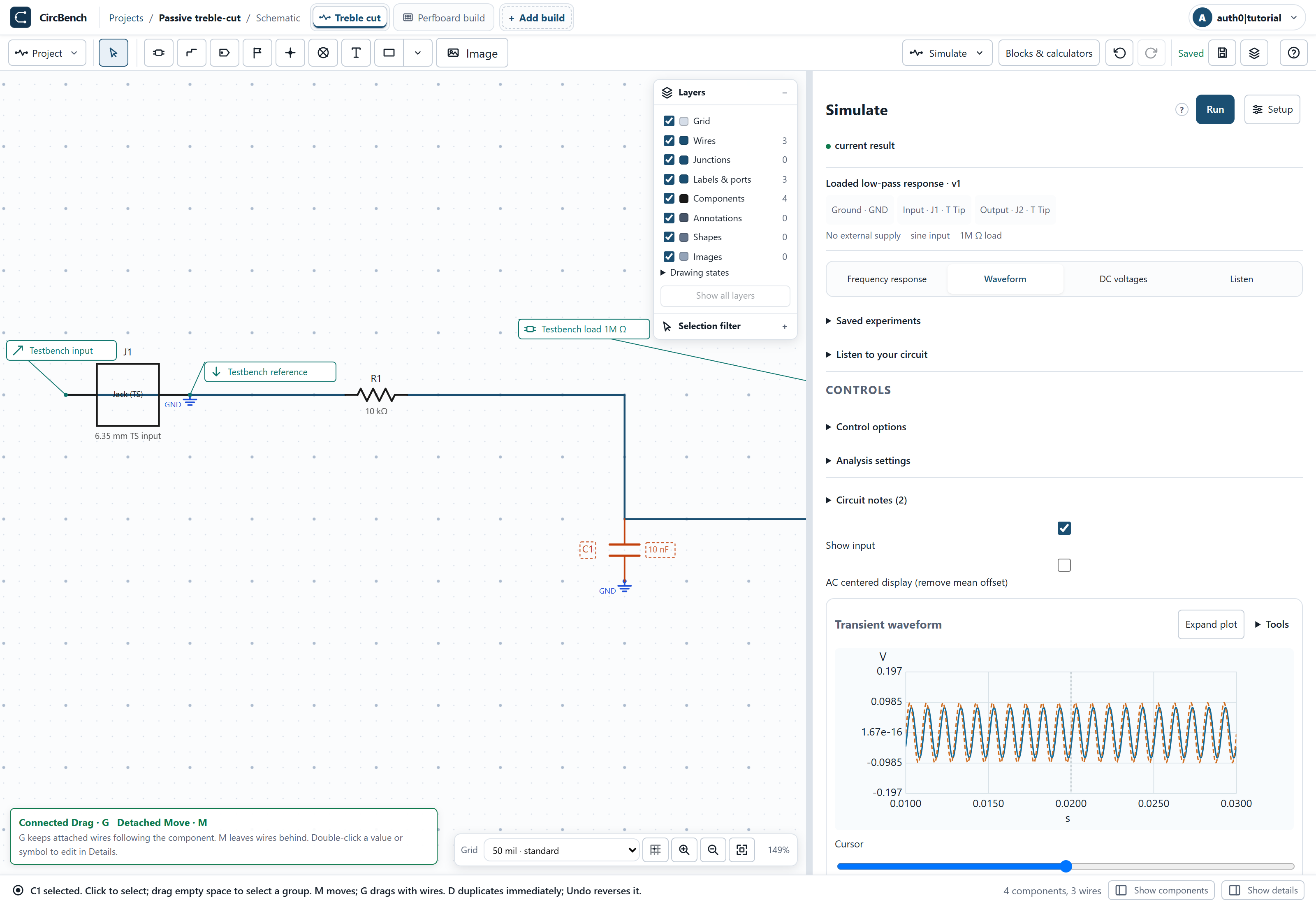
8. Compare input and output waveforms
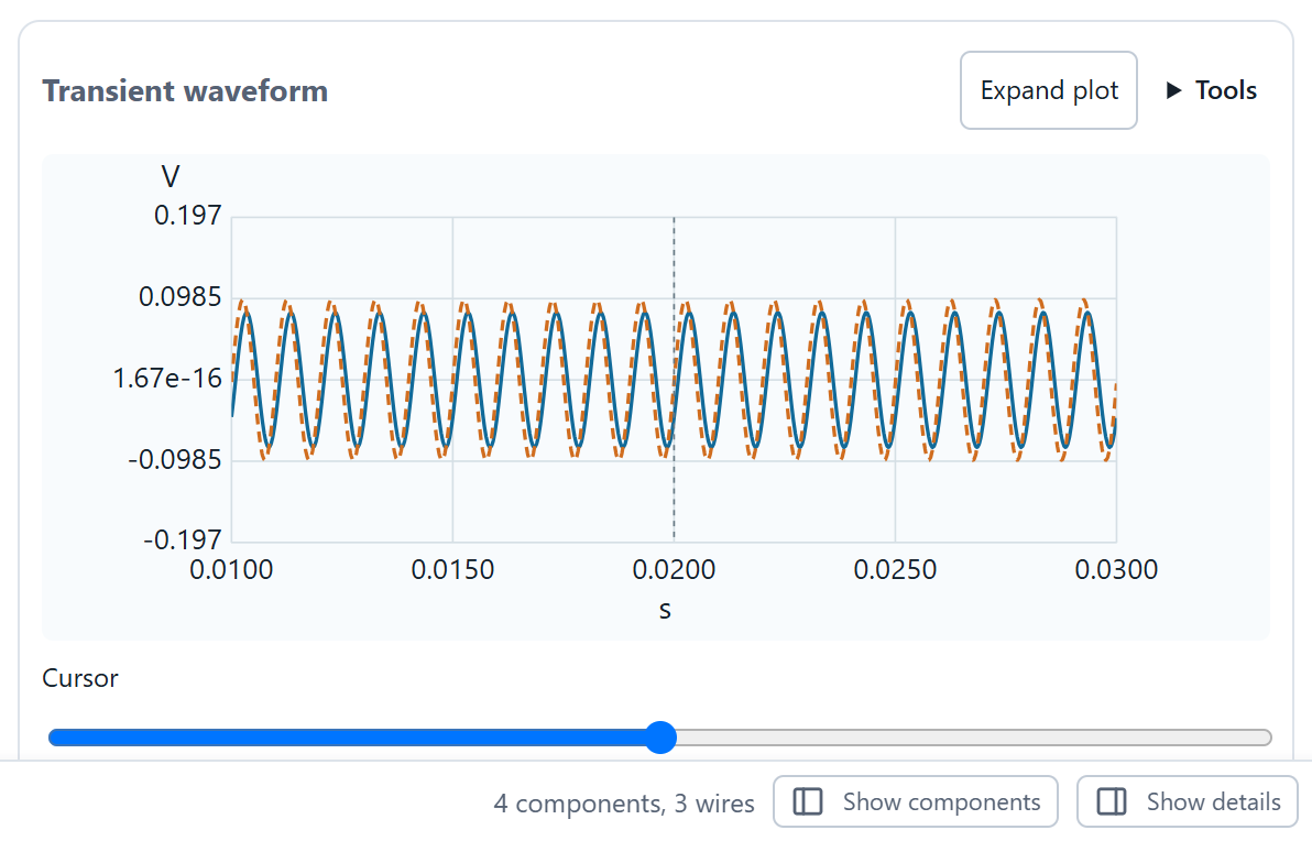
Choose Transient waveform and Run analysis. The dashed input and solid output should be smooth 1 kHz sinusoids, with the output smaller and delayed. Under this explicit bench, output is approximately 82 mV peak for the 100 mV generator. Cursor readings are instantaneous samples, not peak amplitude. Read the settled cycles rather than a single cursor position.
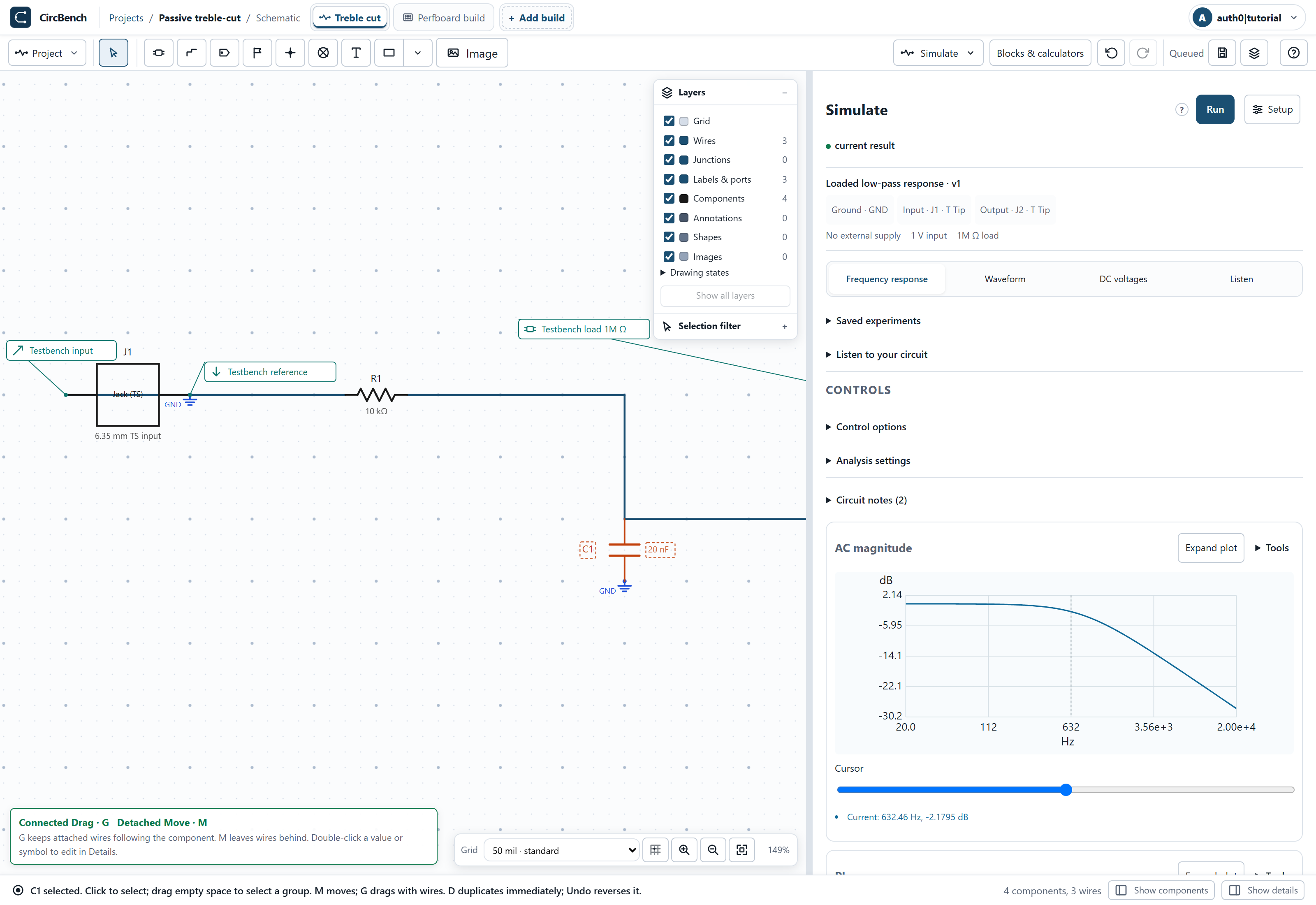
9. Try twice the capacitance
Return to Design, inspect C1 and change Value to 20n. Run a new AC response; the roll-off moves downward, approximately halving the pole. Previous results are stale after an edit. Use Undo to restore 10 nF before following the board guide. A permanent change also requires updating the fitted capacitor value in Builds.
Build the physical layout
10. Orient the perfboard
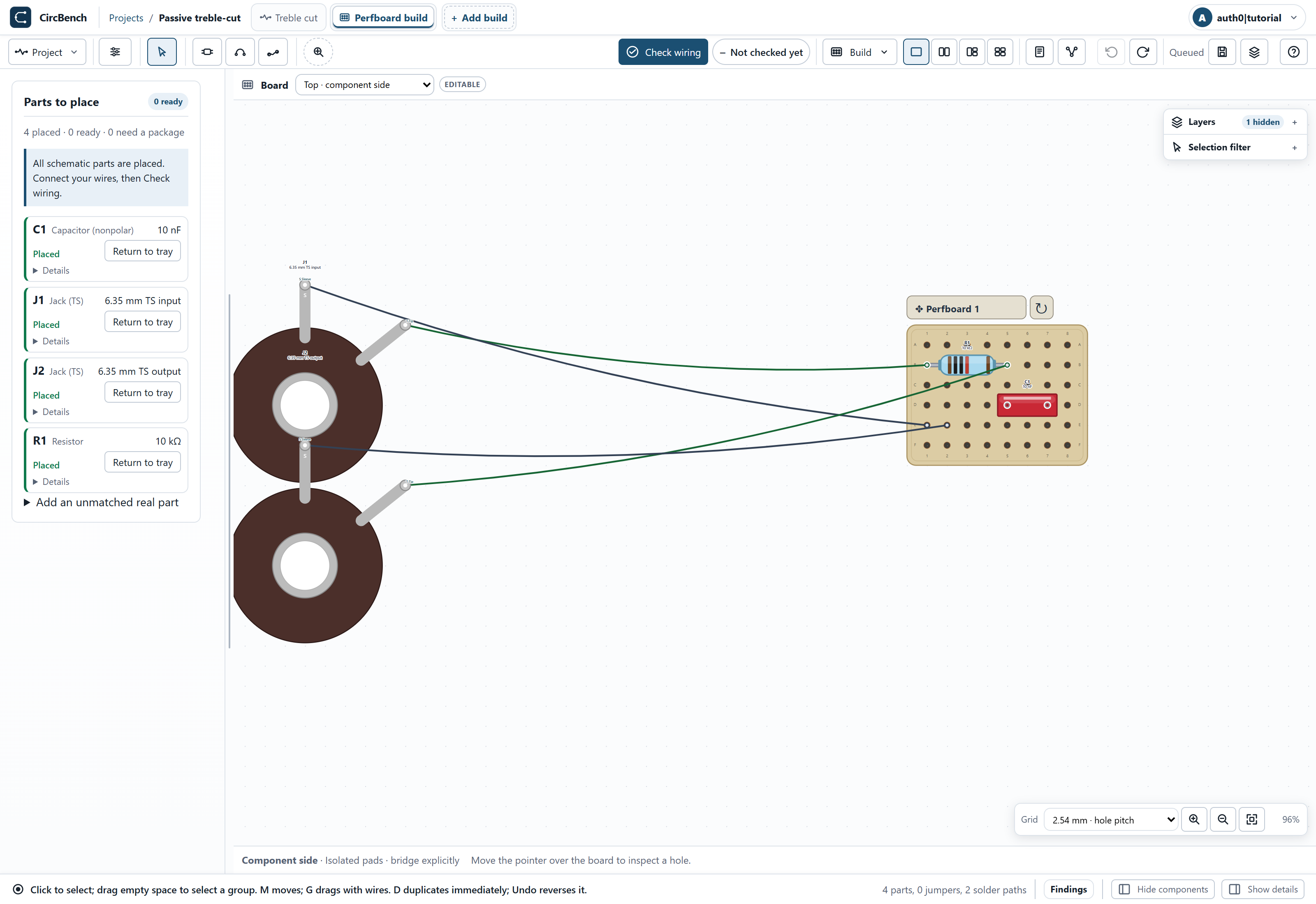
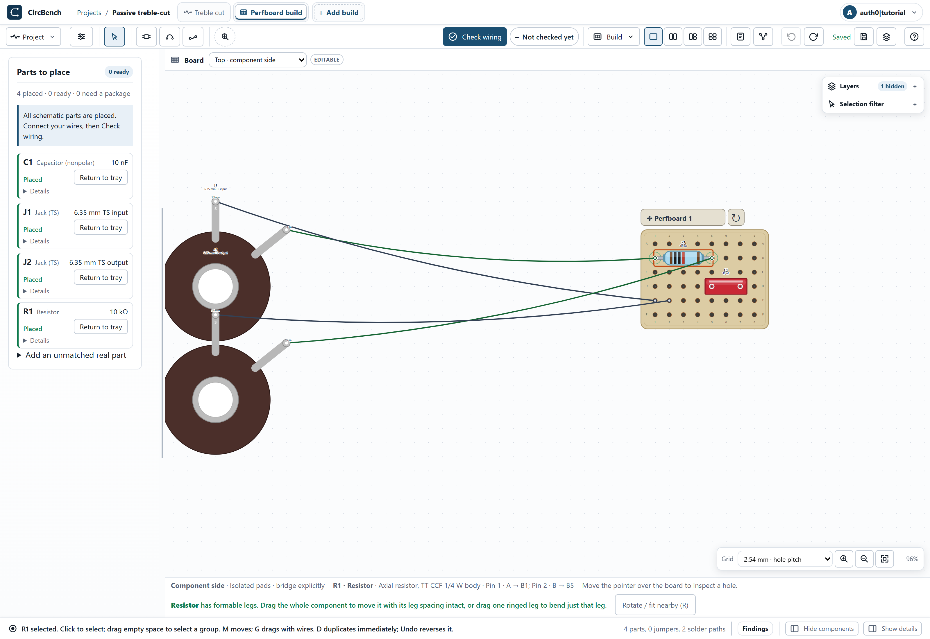
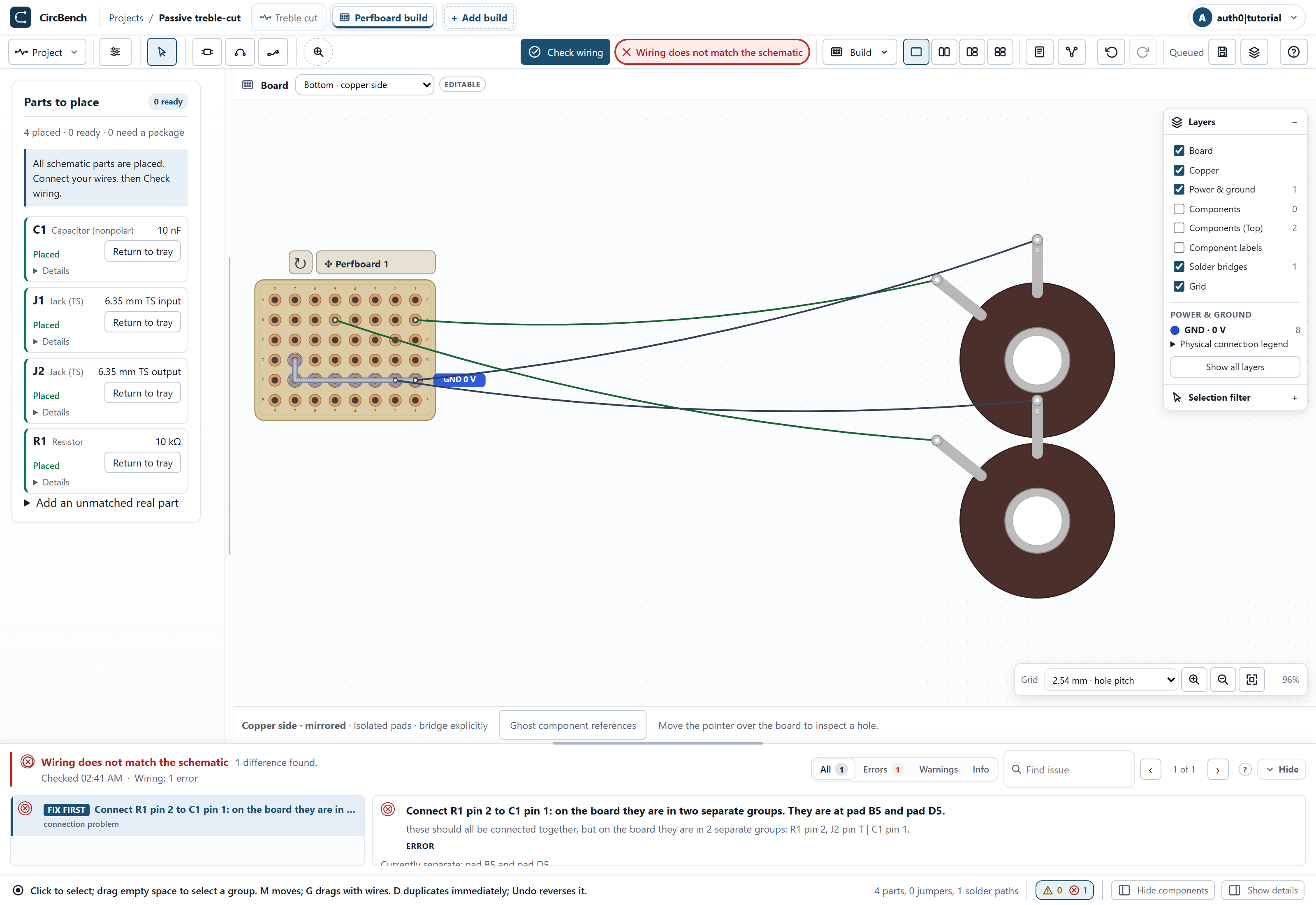
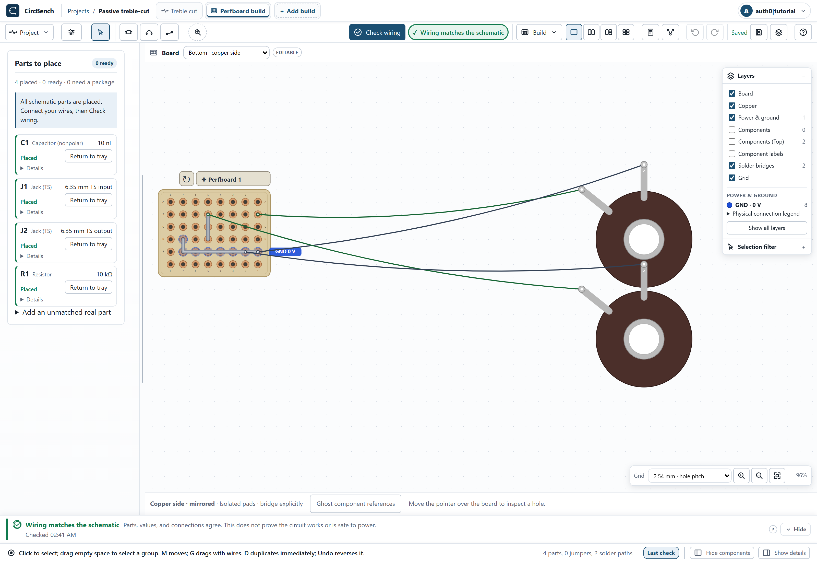
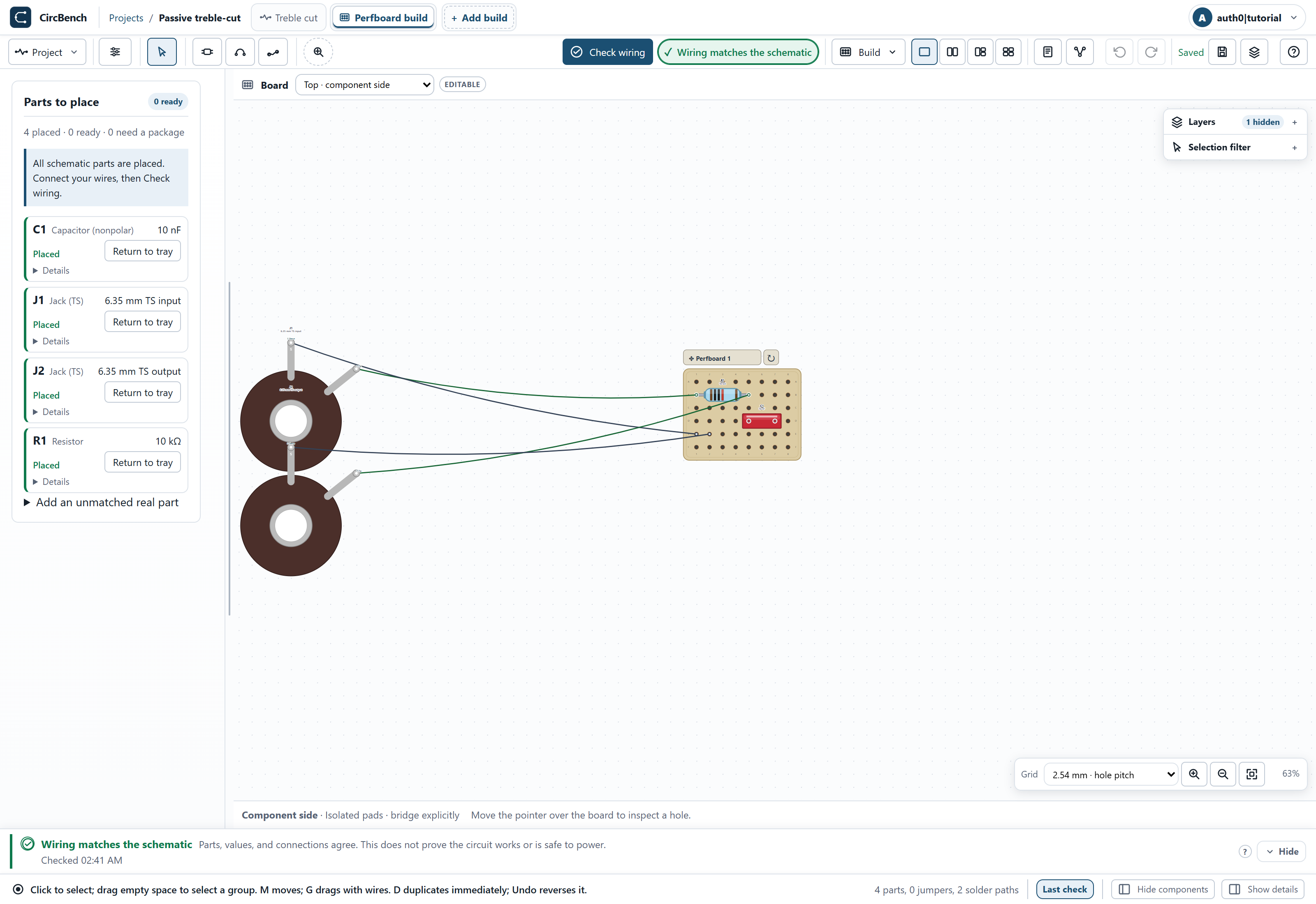
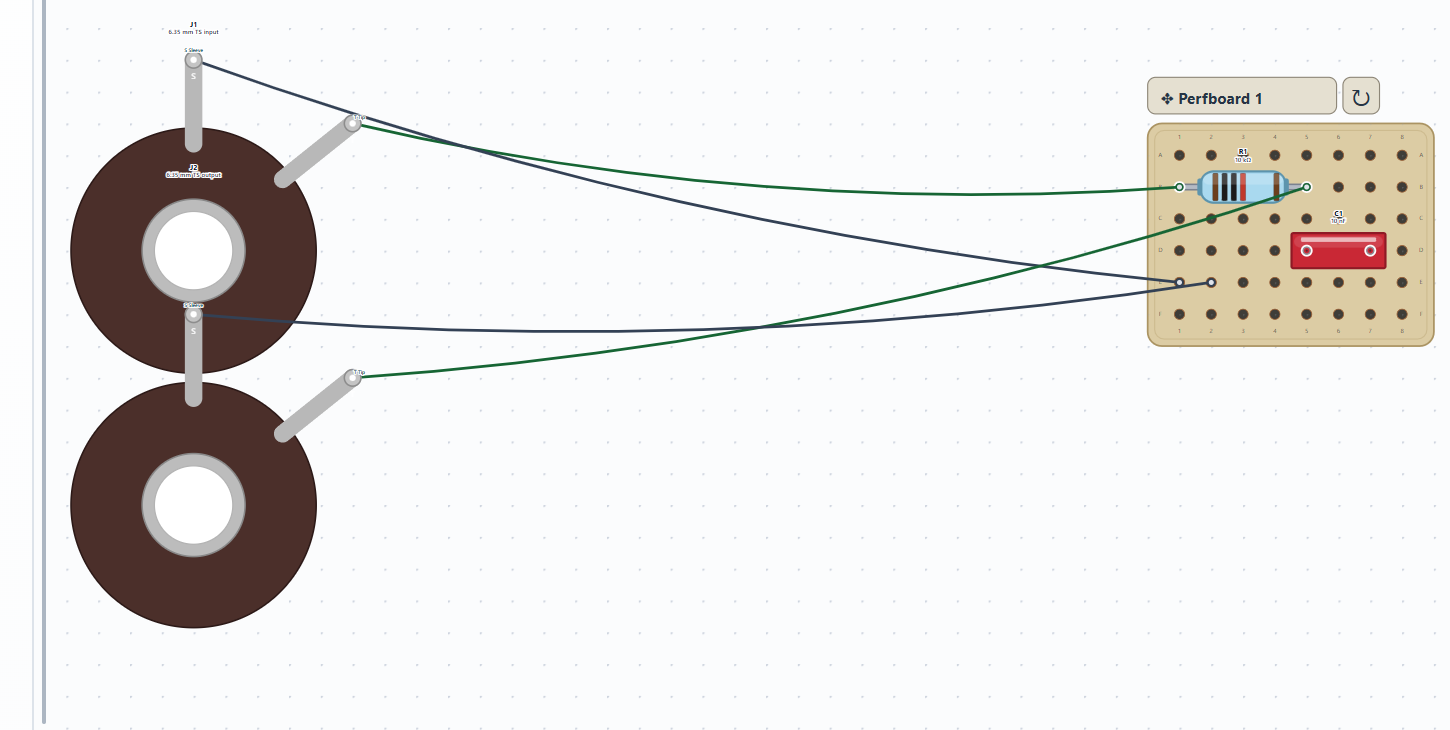
Open the Perfboard build tab and Fit board to window. The reviewed board has eight columns and six rows. Component-side rows A–F correspond to internal rows 1–6; for example r2c5 is B5. Isolated perf pads are separate conductors until an explicit solder path or wire joins them.
11. Place the fitted parts
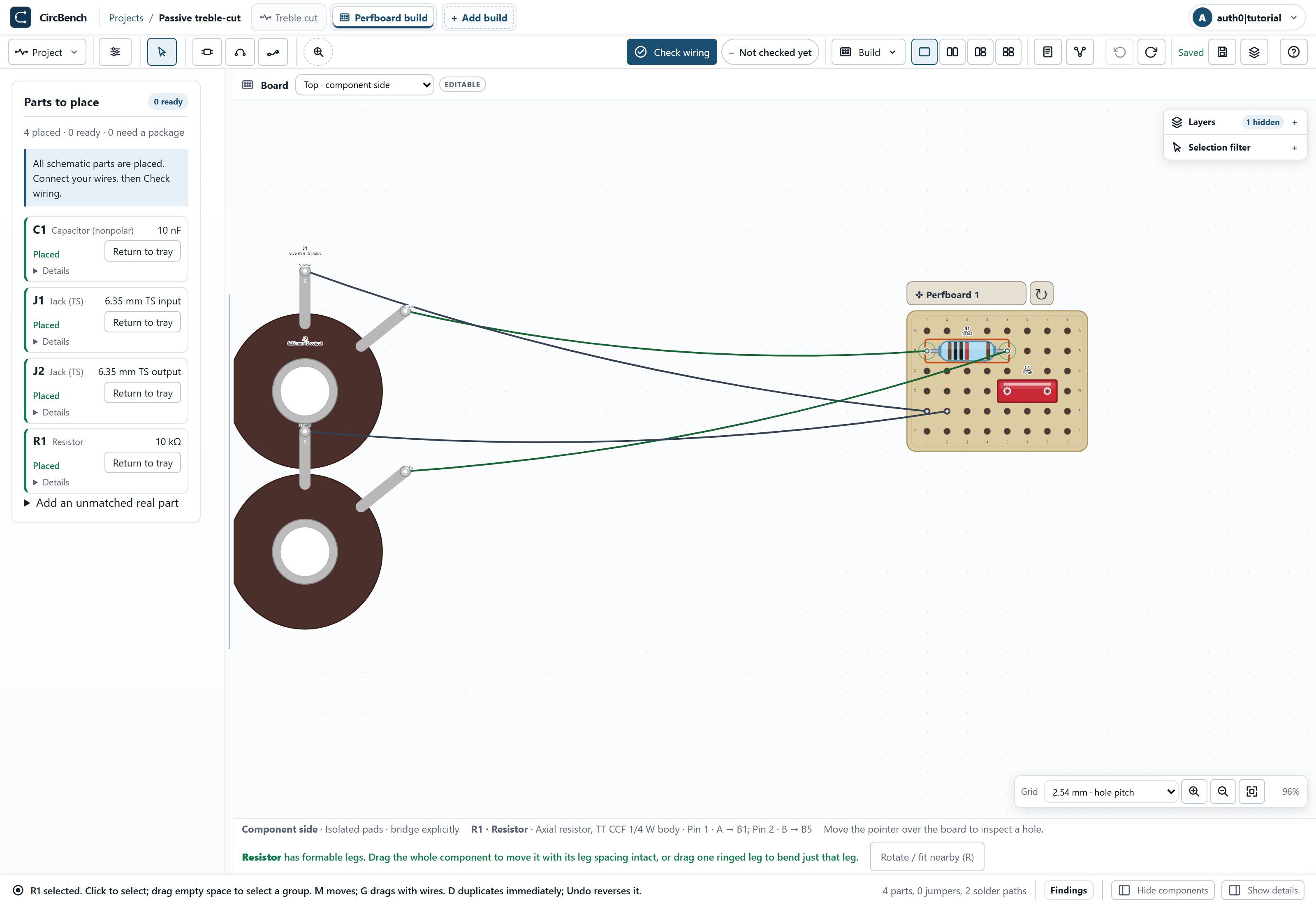
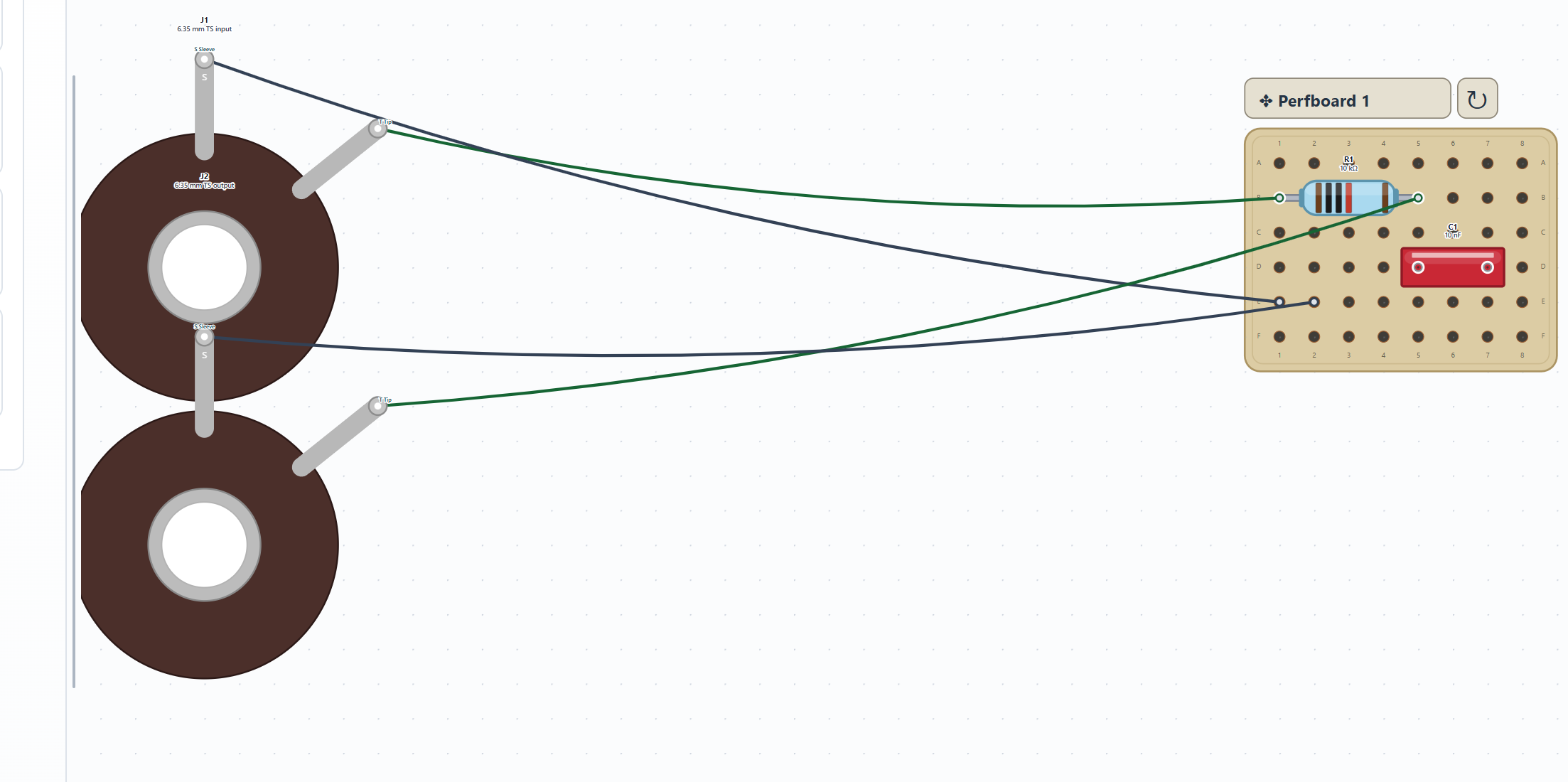
Confirm R1 spans B1–B5 (r2c1–r2c5) and C1 spans D5–D7. Check their fitted values as well as the schematic values. Keep the input side at B1 and the output side at B5. A line passing near a pad does not attach a lead to it.
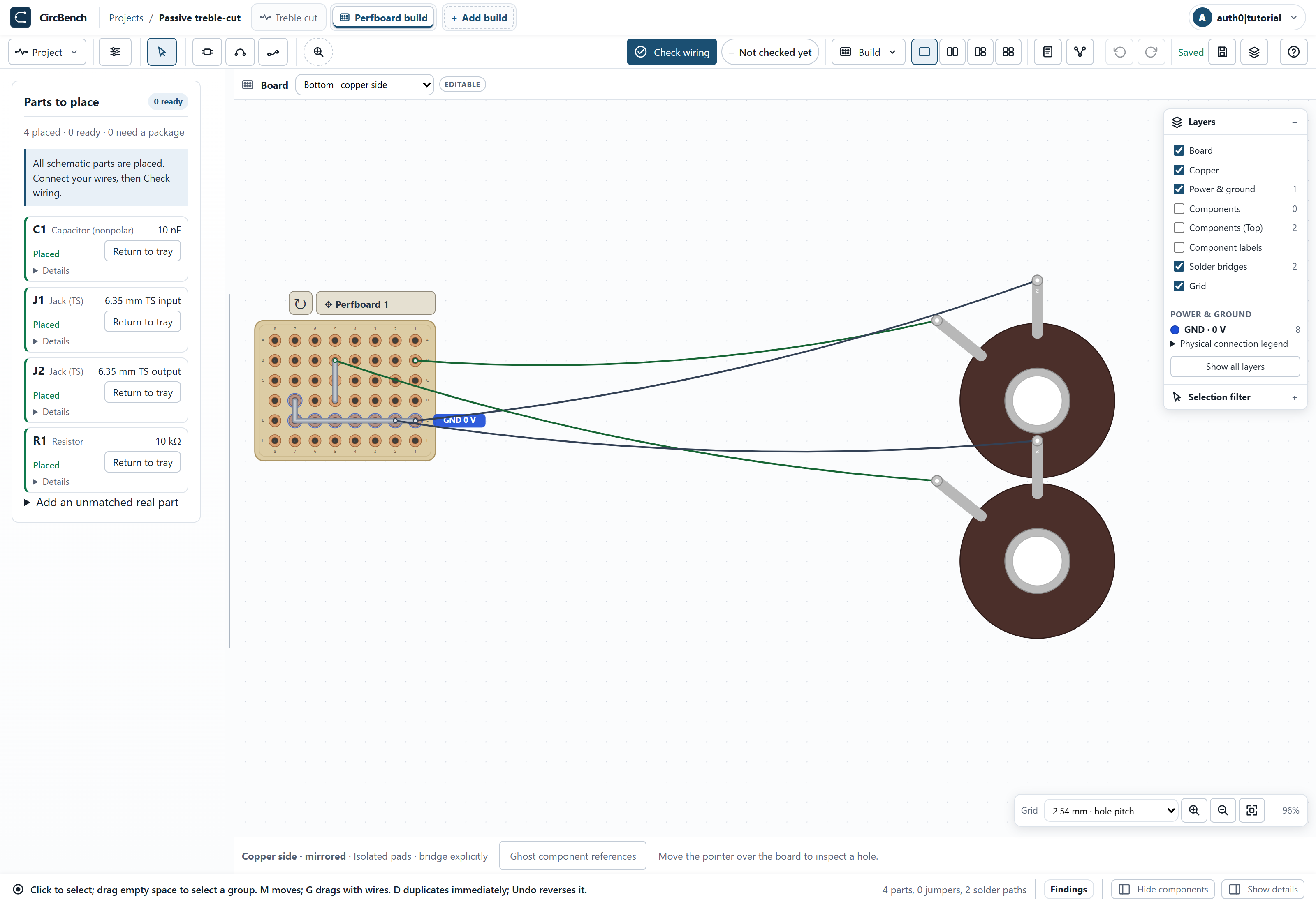
12. Join output and return copper
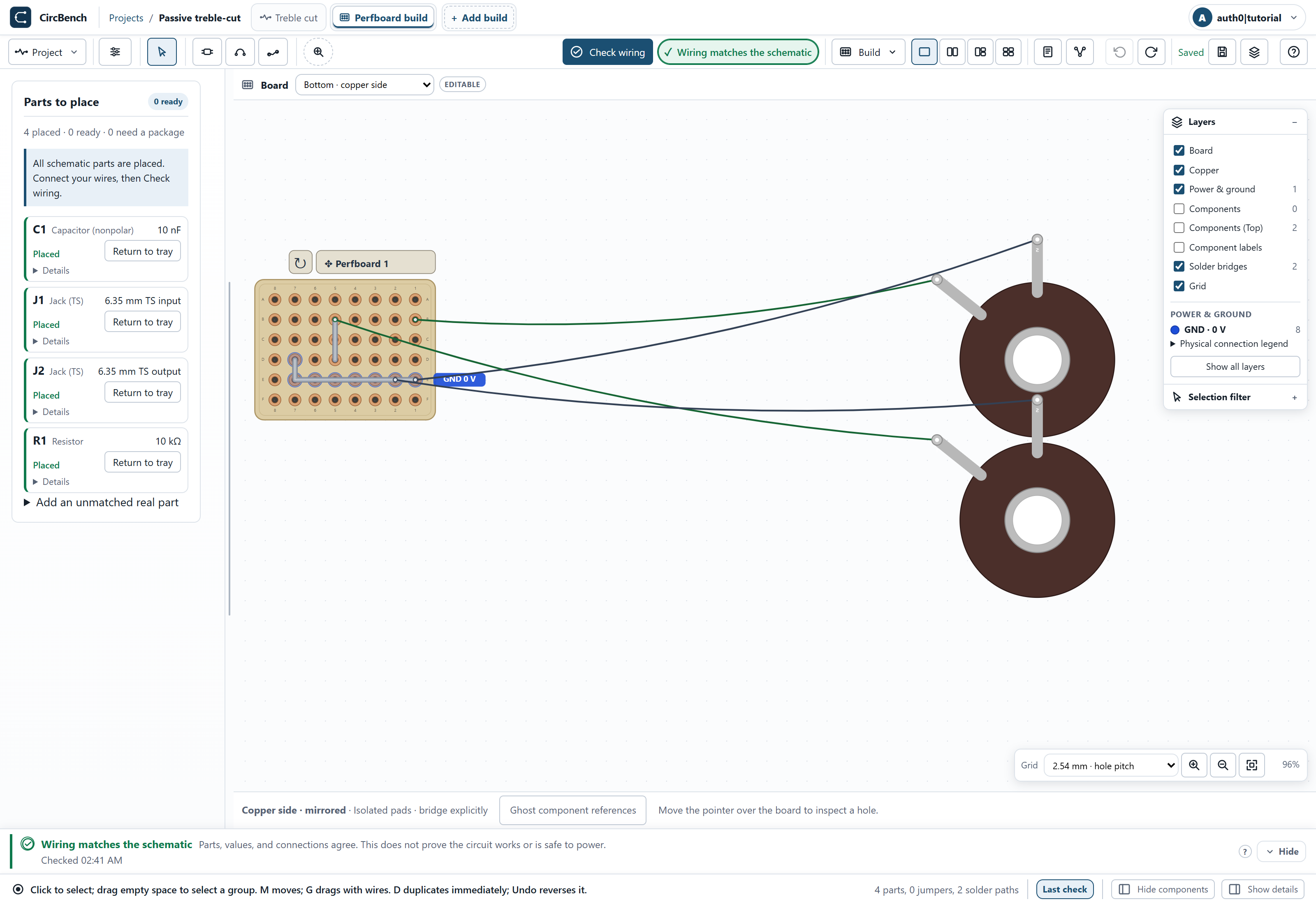
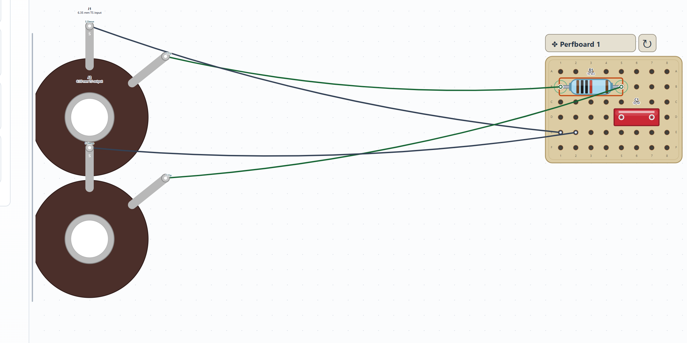
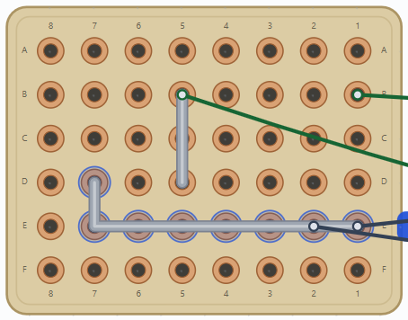
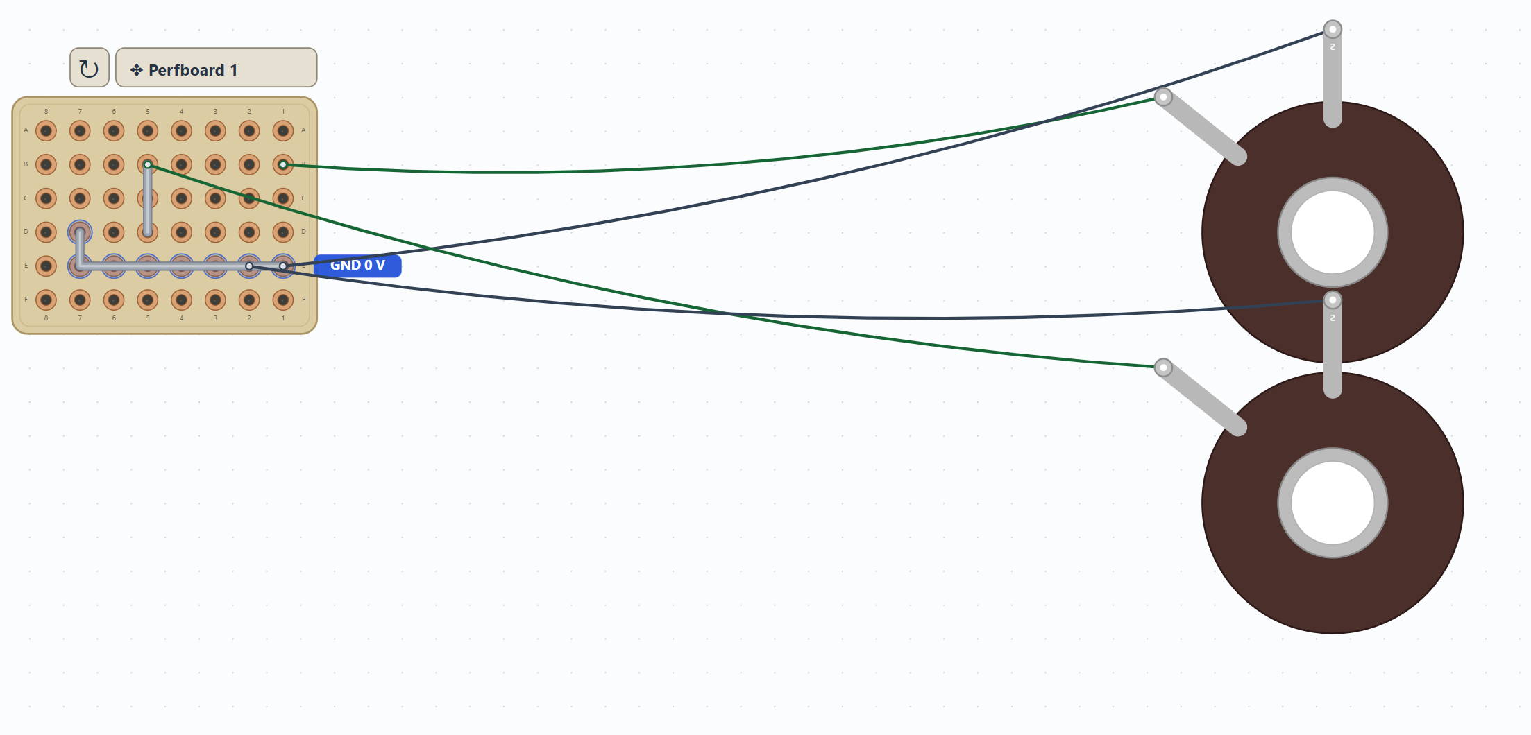
Select the copper face. Add the output solder path B5 → C5 → D5, joining the resistor output to C1. Add the return from D7 through E7 and across row E to E1. The view is mirrored from the component face: follow the printed hole labels rather than counting from the left of the image.
13. Wire the panel jacks
Return to the component face. Connect input tip to B1 and output tip to B5. Input and output sleeves attach to E1 and E2, within the explicit common-return path. The connection schedule below lists the exact reviewed attachments. Jacks are panel hardware, so their terminals are not implicit perfboard pads.
Exact reviewed connection schedule
The following tables come from the same versioned backup. Terminal identities belong to the fitted part; letter/number contacts belong to the board. In the copper view the picture mirrors, but these labels retain their identity.
| Part | Logical terminal → board contact |
|---|---|
| R1 | 1 → B1; 2 → B5 |
| C1 | 1 → D5; 2 → D7 |
| J1 | T → B1; S → E1 |
| J2 | T → B5; S → E2 |
| Insulated connection | Endpoint A | Endpoint B |
|---|
| Solder path | Contacts in order |
|---|---|
| 1 | B5 → C5 → D5 |
| 2 | D7 → E7 → E6 → E5 → E4 → E3 → E2 → E1 |
Check, repair and preserve the project
14. Run a fresh independent wiring check
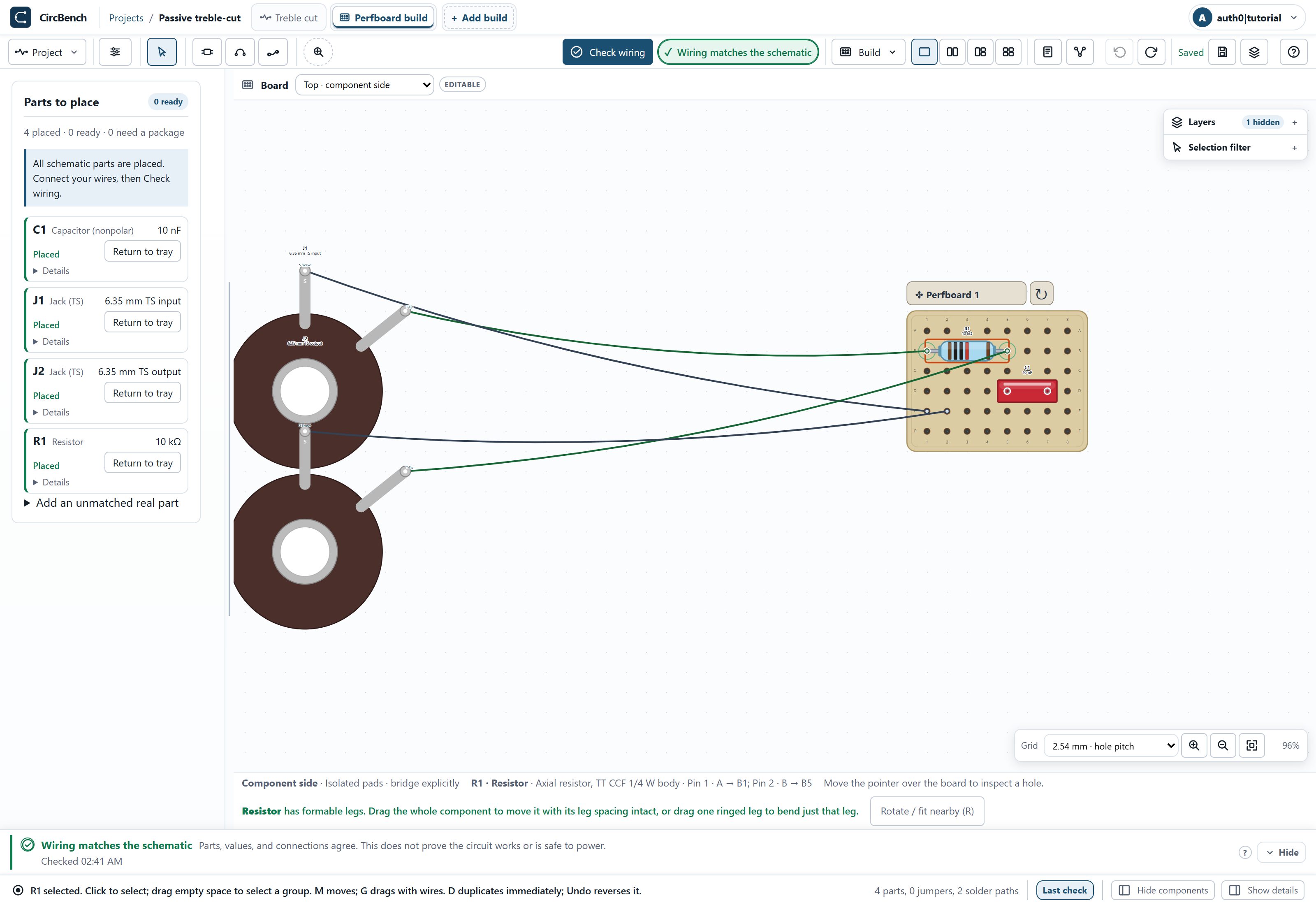
Choose Check wiring and wait for the completed match. CircBench extracts the represented board connections independently and compares them with the schematic. If your copy differs, reveal each reported open or short, verify both endpoints and check unplaced parts or fitted mappings. A previous or pending result is not a fresh match.

15. Introduce a deliberate wiring fault
On the copper face, select and delete the short B5–C5–D5 output solder path in your account copy. Run Check wiring again. The new open separates C1 from the resistor/output node even though the schematic remains intact. Inspect the reported contacts rather than assuming a plausible drawing is electrically connected.

16. Undo the fault and prove the repair
Choose Undo to restore the deleted connection or cut. Run Check wiring again and wait for a fresh match. Undo alone is not verification: the completed check proves the represented topology was restored. Keep this repaired version for the following persistence and download checks.

17. Save, reload and check again
Wait for the normal save indicator, then reload the page. Open the same build and run Check wiring again. Confirm a fresh match after reload. If saving reports a problem, open save recovery and export a backup; do not assume remote account storage succeeded merely because the editor still displays the project.
18. Inspect and export the parts list
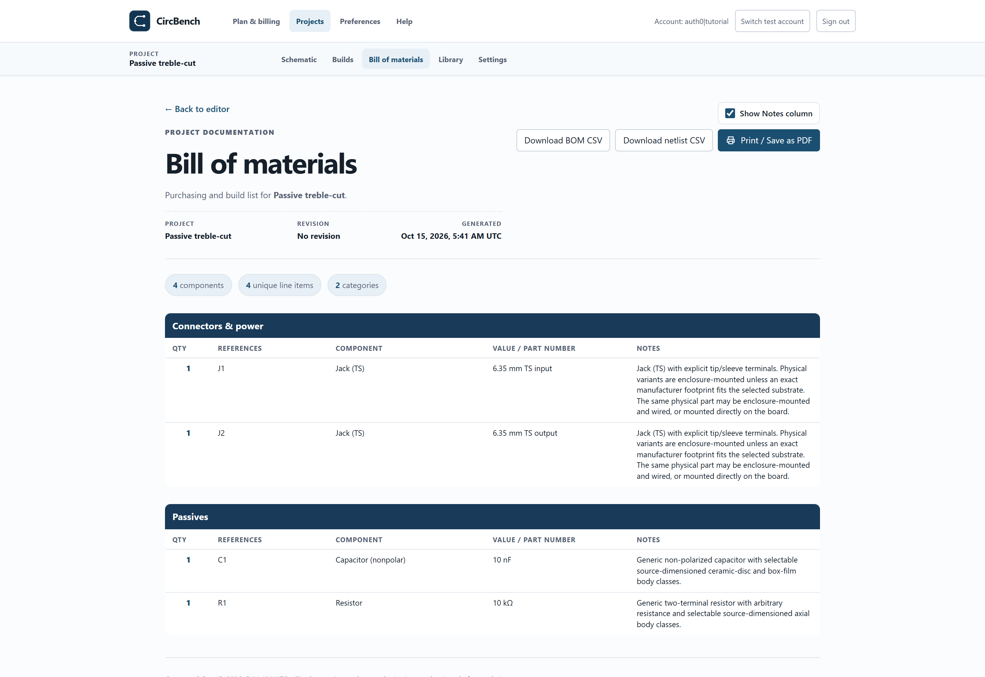
Open Bill of materials, review the fitted parts, values and quantities, then use Export CSV. Compare it with the versioned parts list above. A BOM lists represented parts; it does not select manufacturer voltage ratings or prove that a purchased package has the same terminal order. Resolve substitutions before physical assembly.
19. Export a portable project backup
Open project Settings, go to backup and choose Export project. Keep the resulting .circbench.json file. This preserves the schematic, fitted build, definitions and saved bench/model settings. Raw simulation vectors and uploaded audio are separate outputs and are not retained in this project backup.

20. Import the backup and recheck
Return to Projects and Import the backup file. The imported copy appears in your library; explicitly Open its schematic, then its build. Run Check wiring and confirm a new match. If an import is rejected, keep the original file and compare its schema/version with the app rather than editing integrity fields by hand.
What this result establishes
This authored RC teaching circuit does not model a guitar pickup’s frequency-dependent source impedance, enclosure, bypass switch, component tolerances or input protection. The current waveform is a simulation, not an oscilloscope measurement.
The screenshots show current solver results and fresh wiring checks for this exact example version. They do not assert that hardware was assembled, measured or qualified. Use the supplied source, load and stimulus settings when comparing results.
The circuit and layout are CircBench-authored teaching examples. The standard RC concept is also explained in Texas Instruments’ RC circuits training; TI did not design or endorse this build.
Your next project
Compare source loading in the two-input passive mixer, then add gain with the breadboard transistor boost.