breadboard · intermediate
Build a single-transistor guitar boost on breadboard
Draw a 2N5088 boost, inspect DC bias and clipping, and follow a checked breadboard layout with exact jumpers, clear screenshots and downloads.
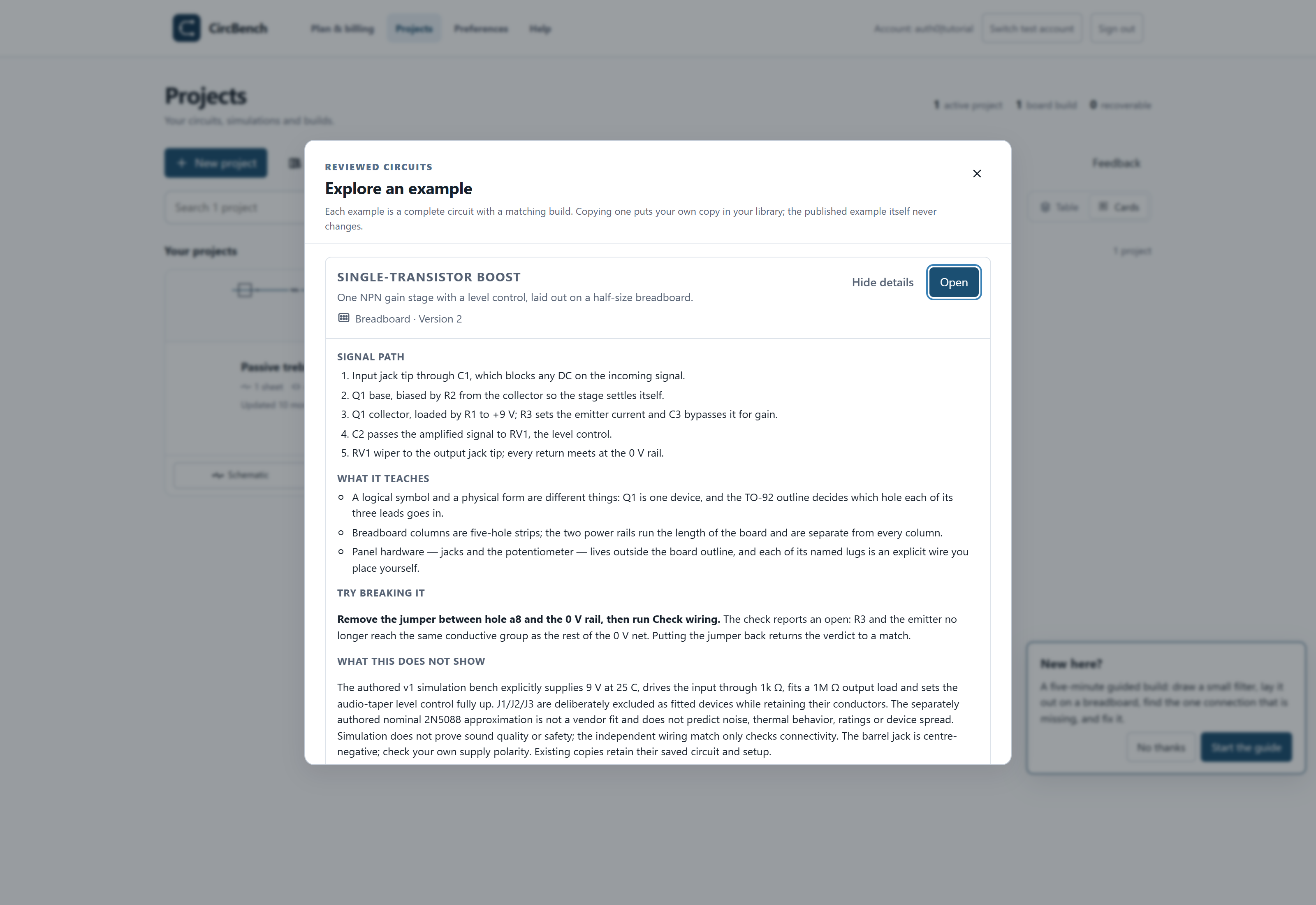
The app opens the current example chooser. Choose Open to create your own account copy. For this guide's exact v2, download and import the project backup if the catalog version has changed.
A common-emitter transistor stage teaches two different questions: where does it sit at DC, and how much signal can it amplify before the waveform changes shape? This guide uses a collector-feedback 2N5088 stage and a complete half-size breadboard layout. Start with a small signal, then deliberately overdrive it.
Parts: Q1 2N5088; R1 10 kΩ, R2 430 kΩ, R3 390 Ω; C1/C2 100 nF, C3 47 µF emitter bypass, C4 100 µF supply filter; A100K level control; TS audio jacks and DC hardware. Confirm all package/polarity mappings in the BOM.
Before starting: have a CircBench account and use a copy for experiments. This is a software build and simulation walkthrough; the images are actual application screenshots, not photographs of assembled hardware. Every numbered step has a detail image and a link to its unmodified full context PNG. Open full size when comparing small pin labels, especially on a phone.
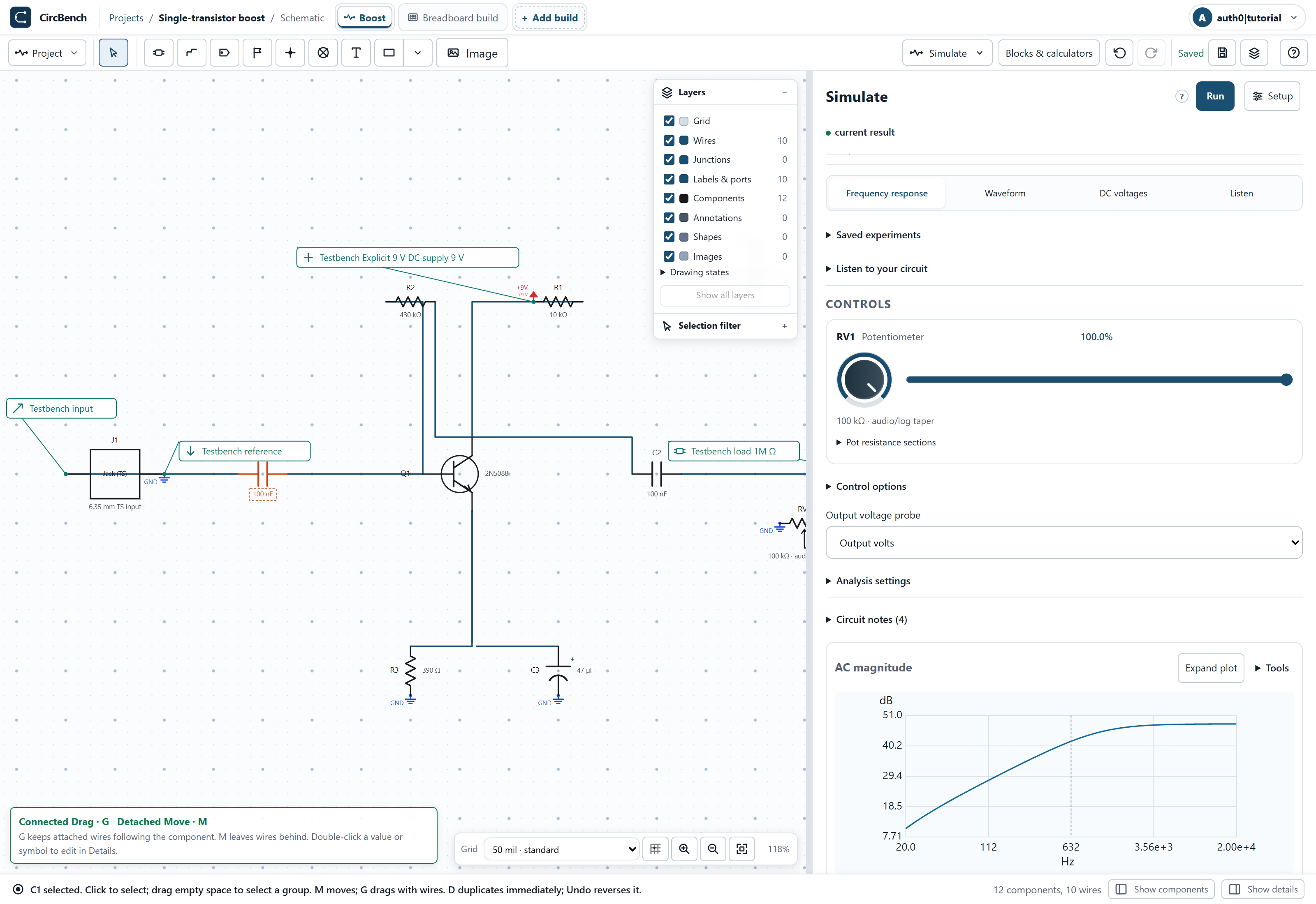
Draw and understand the schematic
1. Open the exact reviewed example
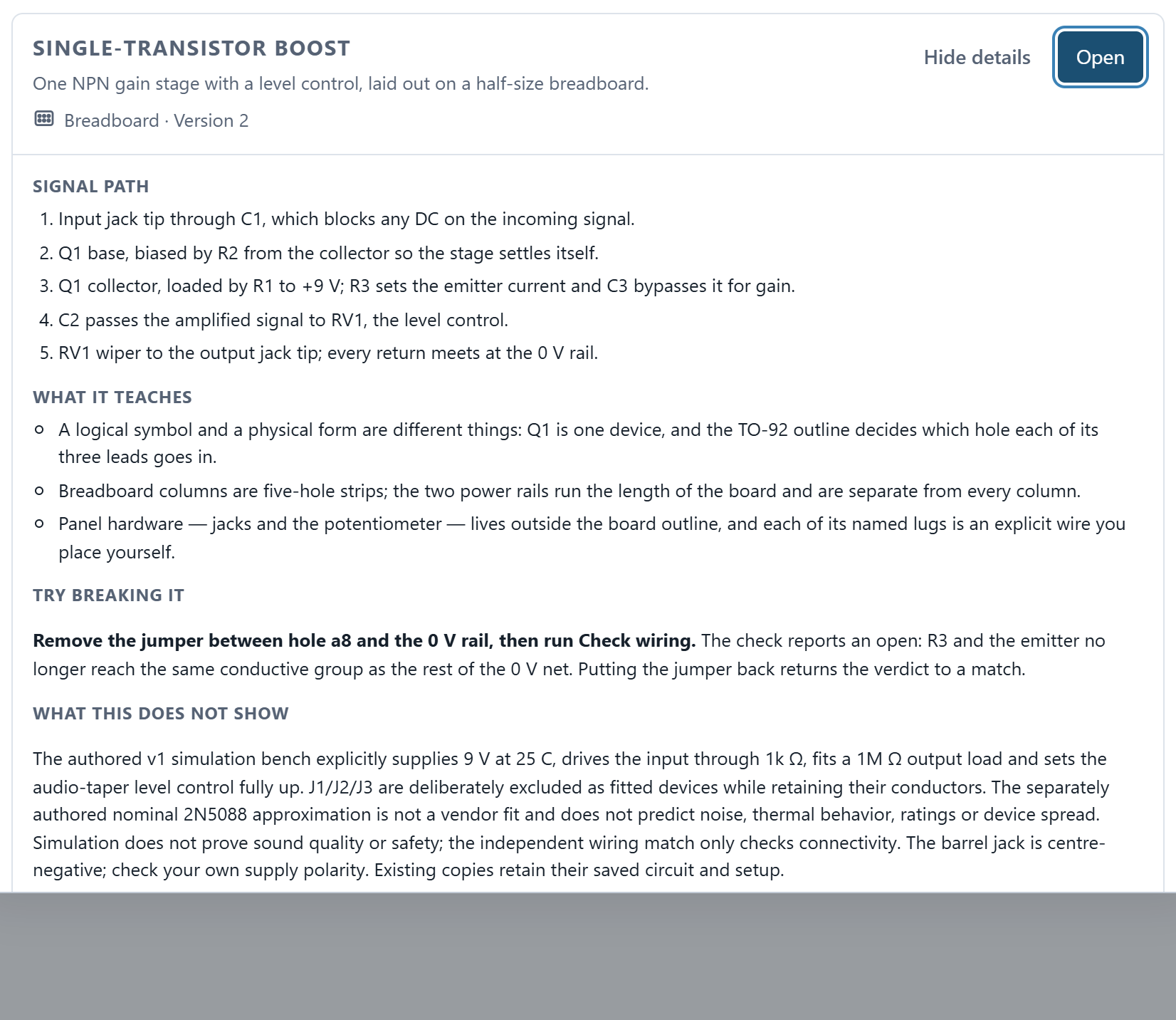
Use the example link above, sign in if requested, and confirm Single-transistor boost, version 2 in Explore an example. Choose Open to create your own account copy. The link alone does not create a project. If the catalog changes, import the versioned backup above to follow this precise guide. All screenshots show the actual reviewed copy, with completed wiring as a reference for your own drawing.
2. Identify the transistor terminals
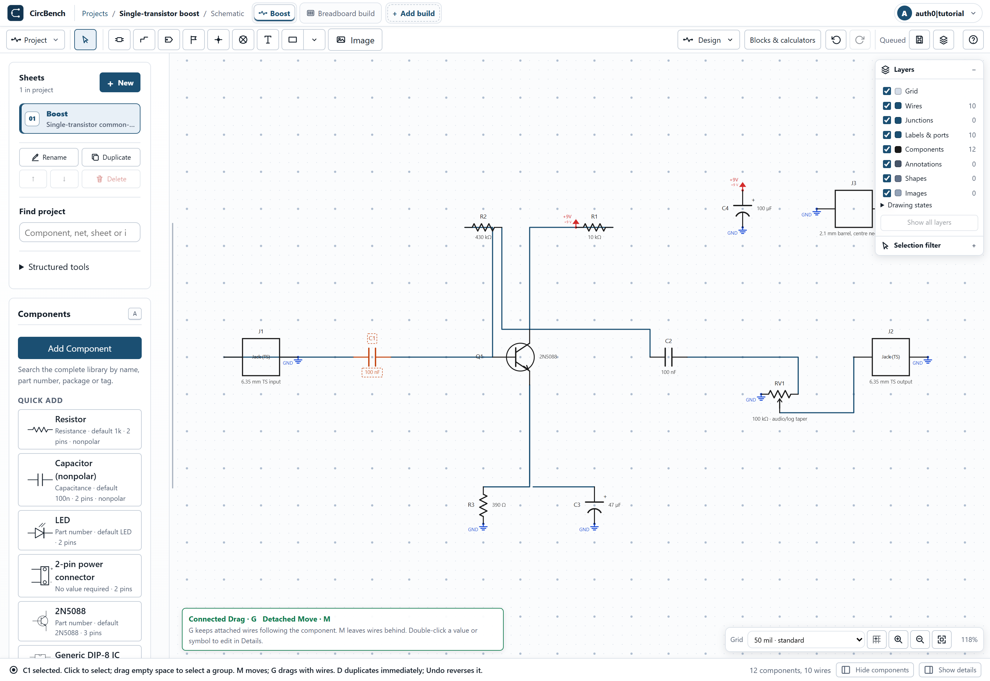
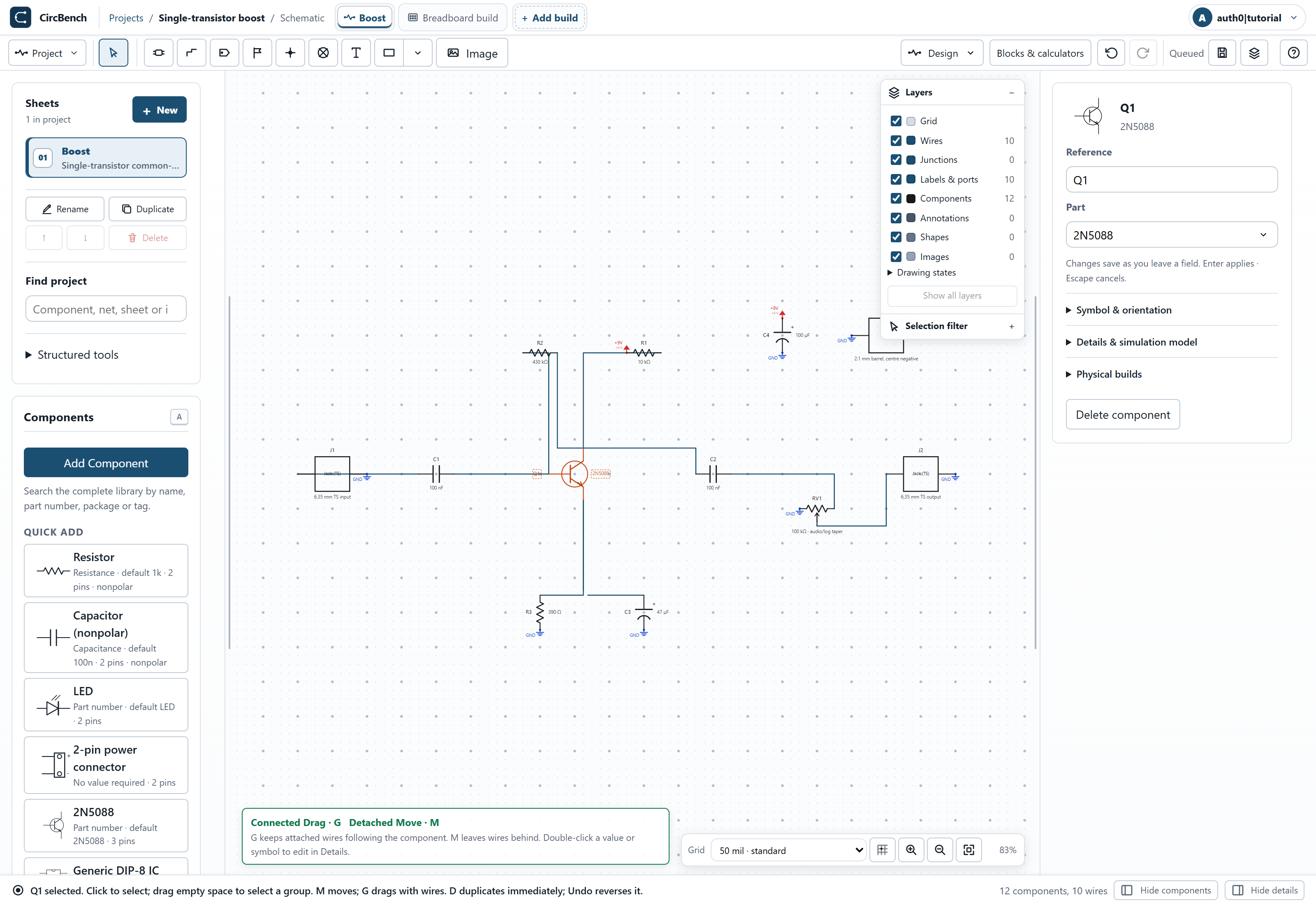
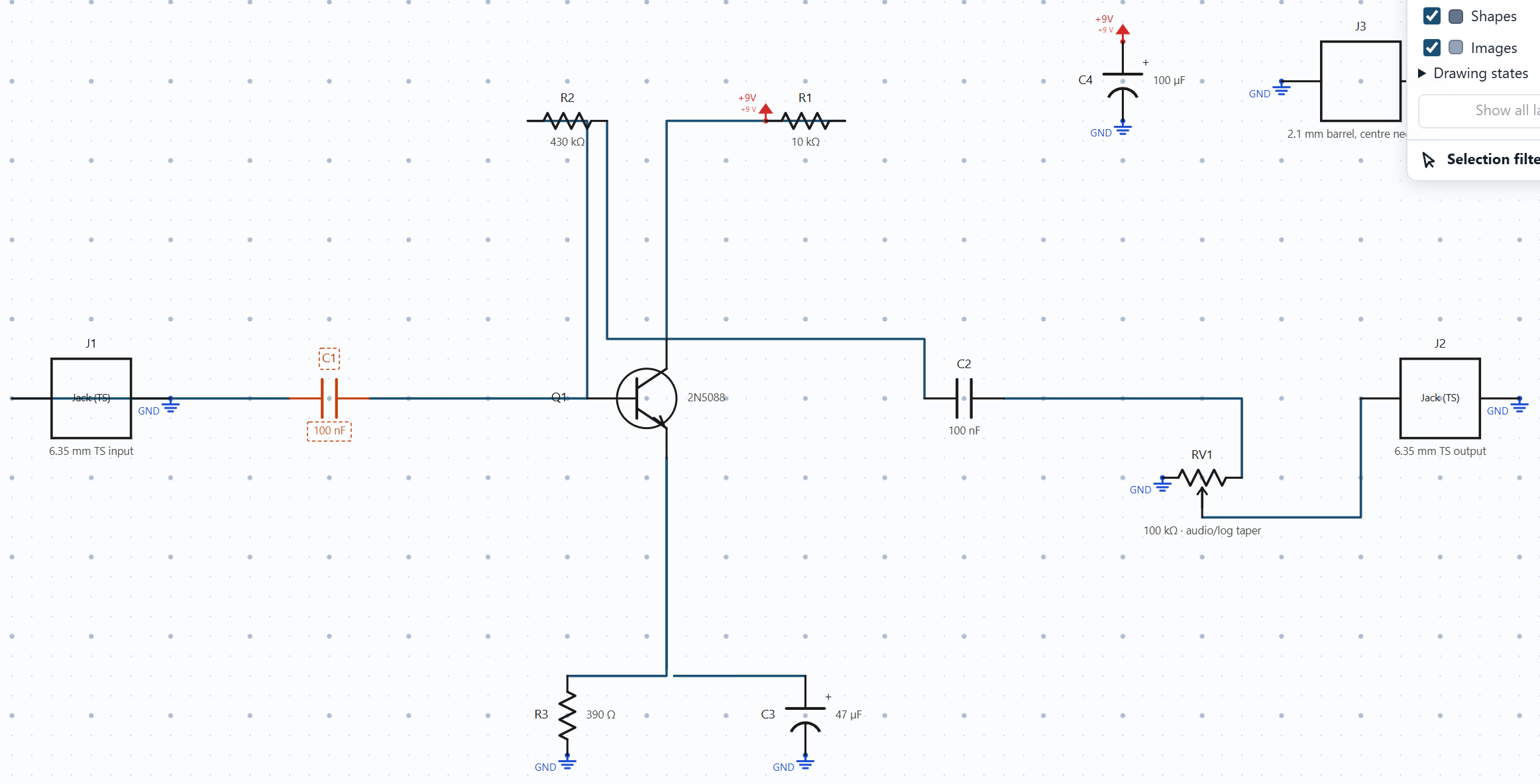
In Schematic, double-click Q1. Confirm the selected device is 2N5088 and identify E, B and C on its symbol. Begin a redraw with Q1, the collector resistor to the supply, the feedback resistor from collector to base, and the emitter resistor to return. Use logical pin identities; a flat-face package assumption cannot establish pin order.
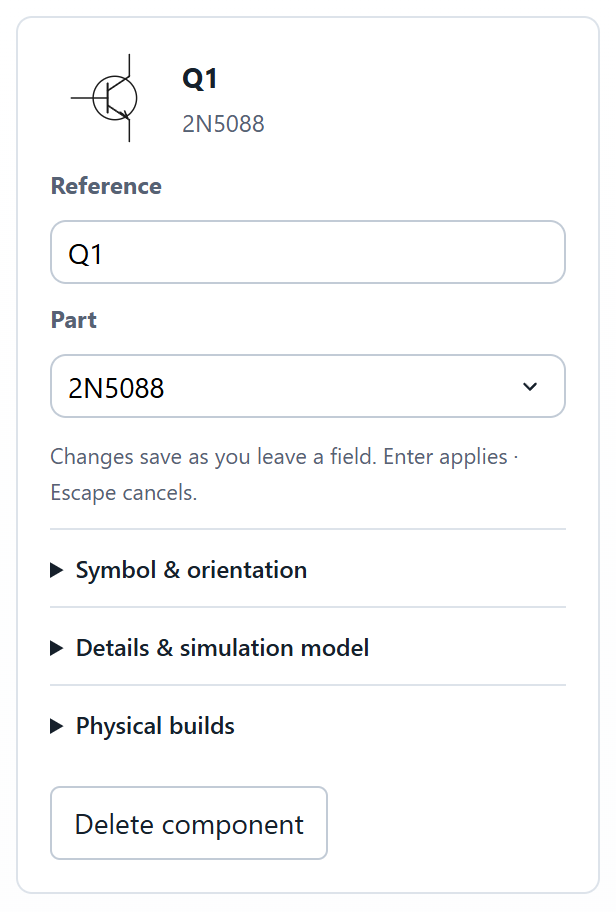
3. Build the bias and coupling network
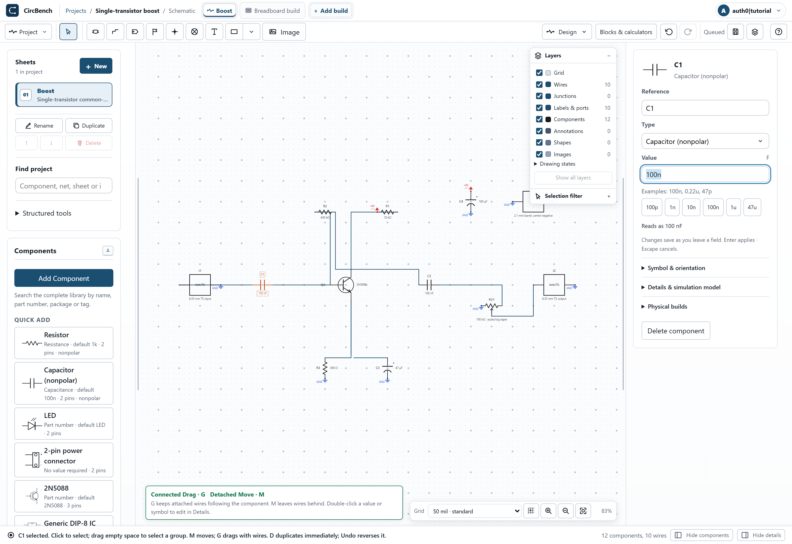
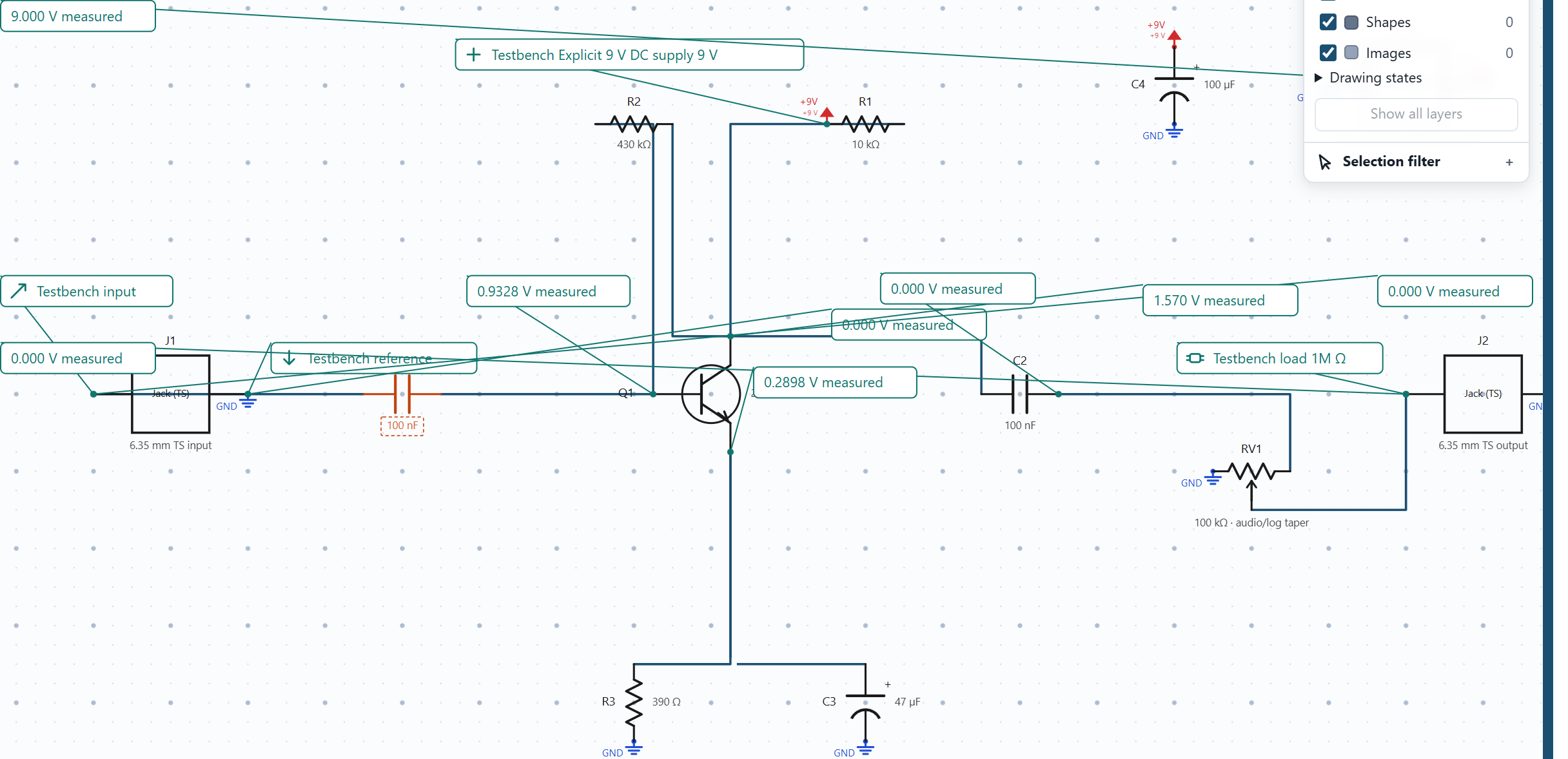
Inspect C1 and confirm 100 nF. Connect input tip through C1 to Q1 base. R1 is 10 kΩ from 9 V to collector, R2 is 430 kΩ collector-to-base, and R3 is 390 Ω emitter-to-return. Add C3, 47 µF, across the emitter resistor with its positive terminal toward the emitter.
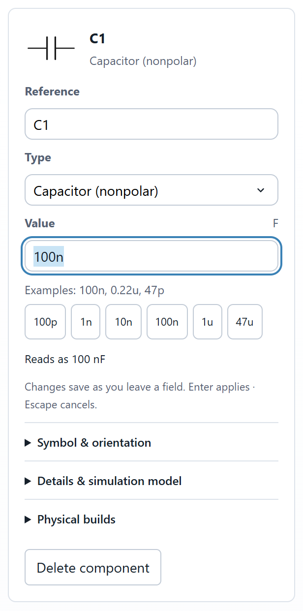
4. Complete the signal and power paths
Fit the full schematic. Couple the collector through C2, 100 nF, to the top of the A100K level track; connect its bottom to return and wiper to output tip. Add C4, 100 µF, across supply/return with correct polarity. Join jack sleeves to return. Coupling capacitors separate stage bias from external signal connections.
Configure and interpret the simulation
5. Select the 9 V bench and model
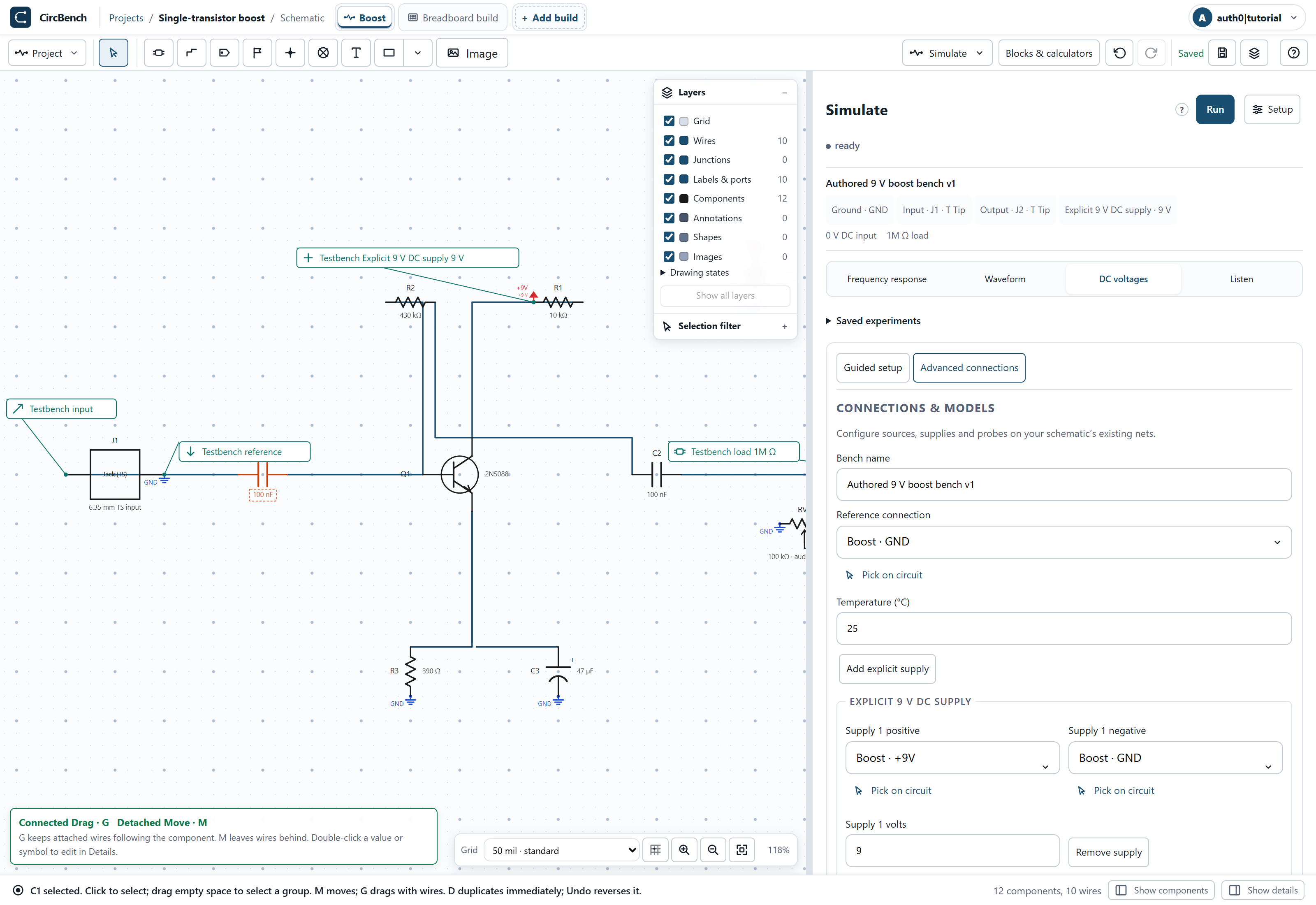
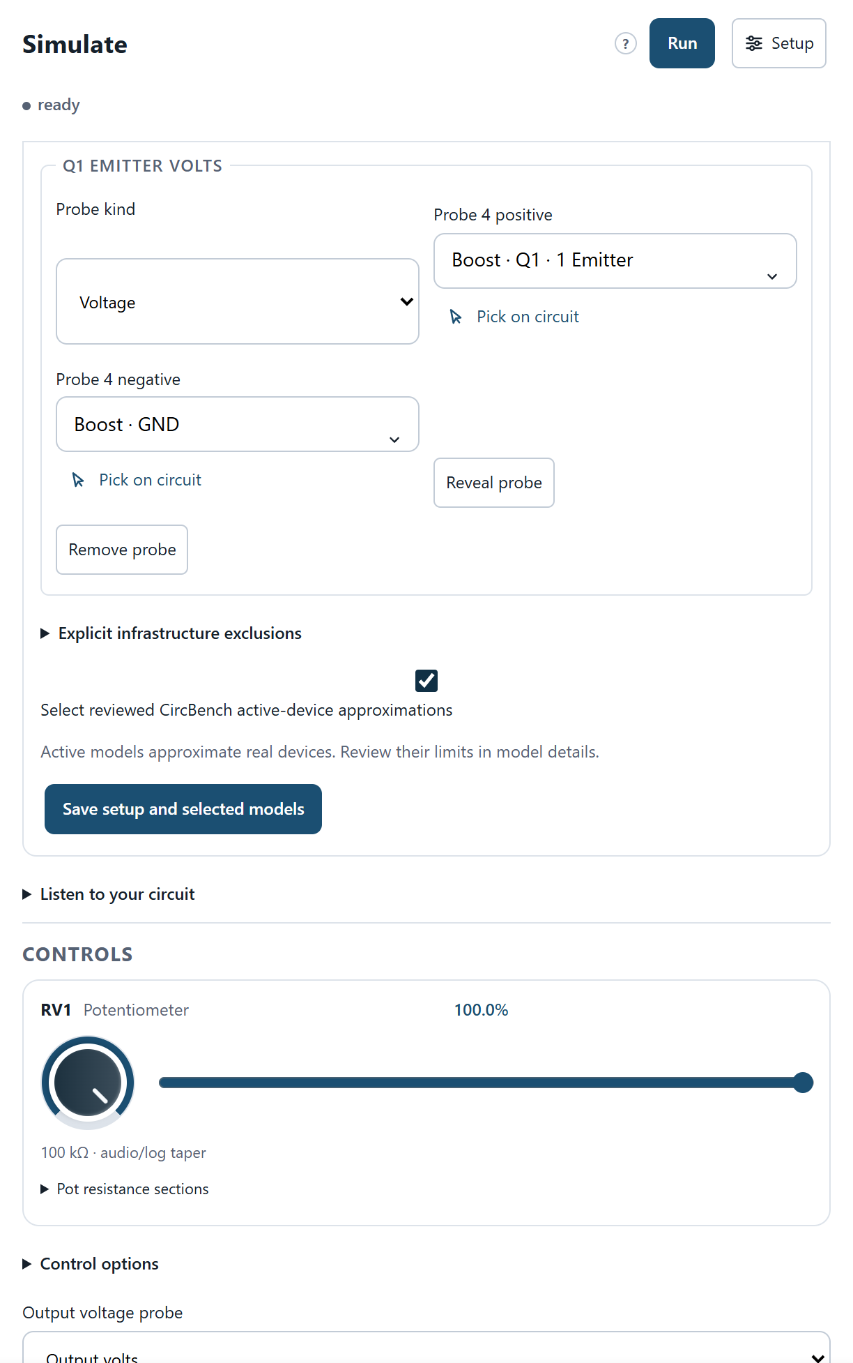
Choose Simulate → Setup. Keep the explicit 9 V supply, 1 kΩ source, 1 MΩ load, full level, 25 °C and 1 mV-peak 1 kHz sine. Verify input, output and reference endpoints. Deliberately select the reviewed CircBench active-device approximation and Save setup and selected models. A supply flag on a drawing alone does not create this test supply.
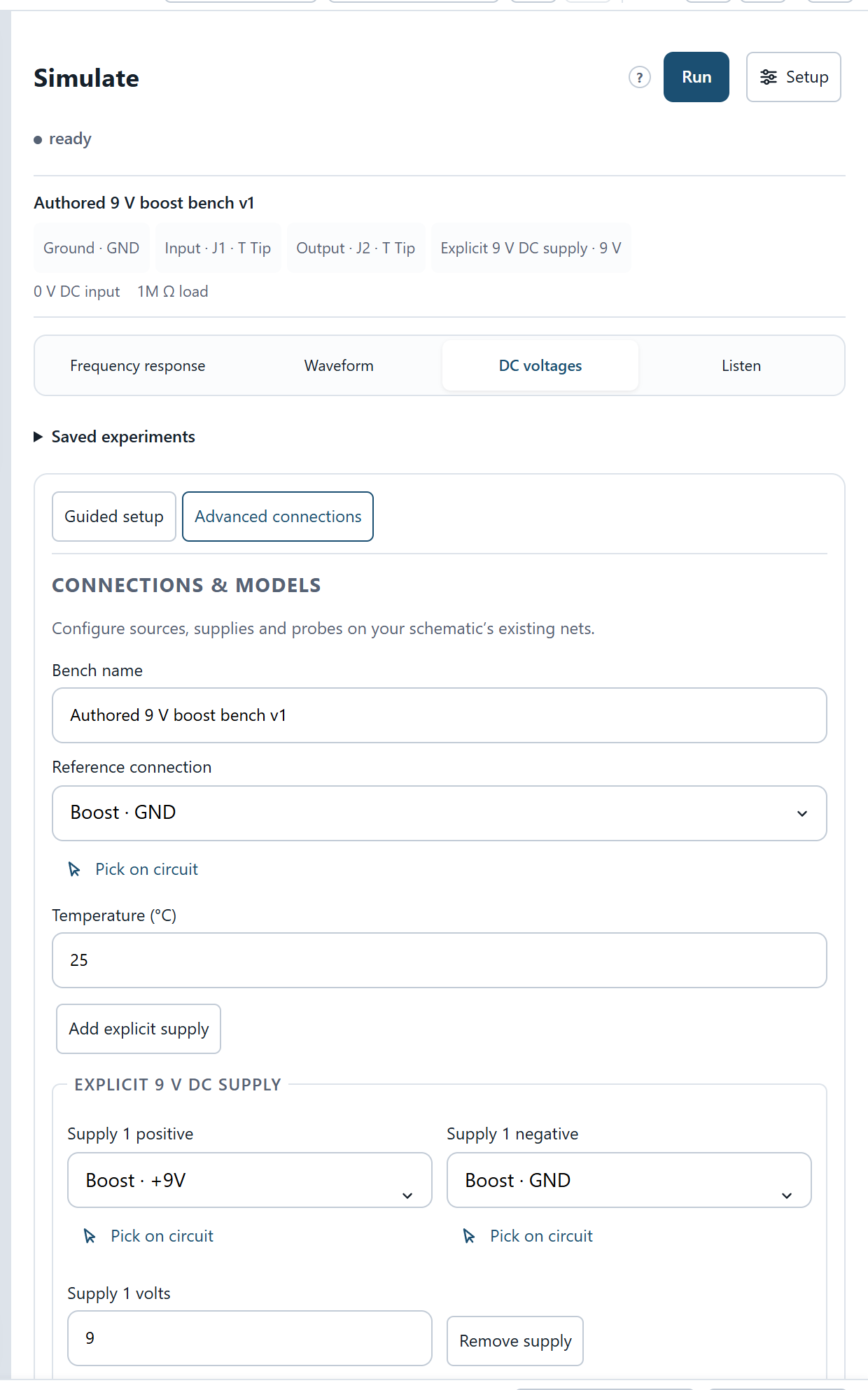
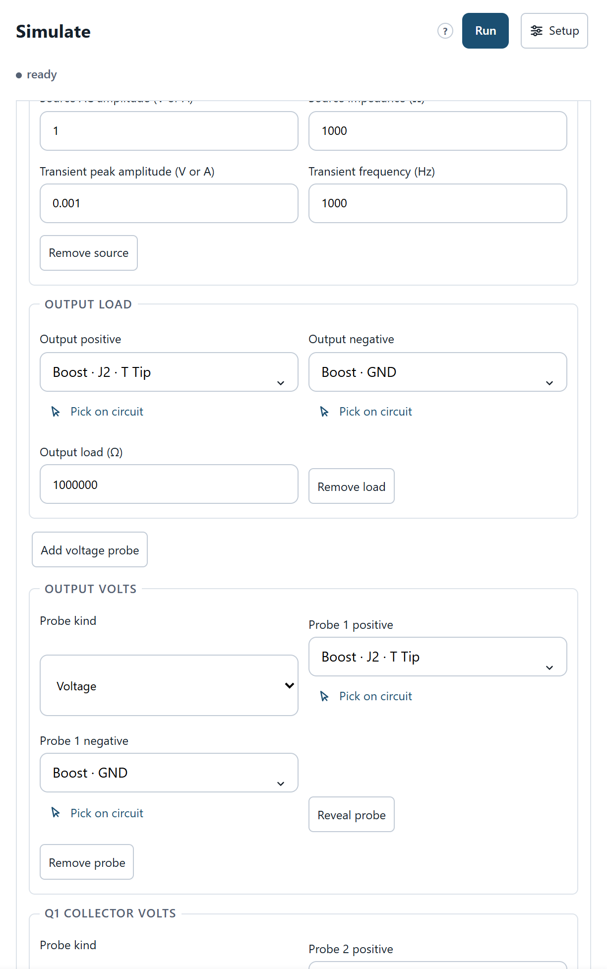
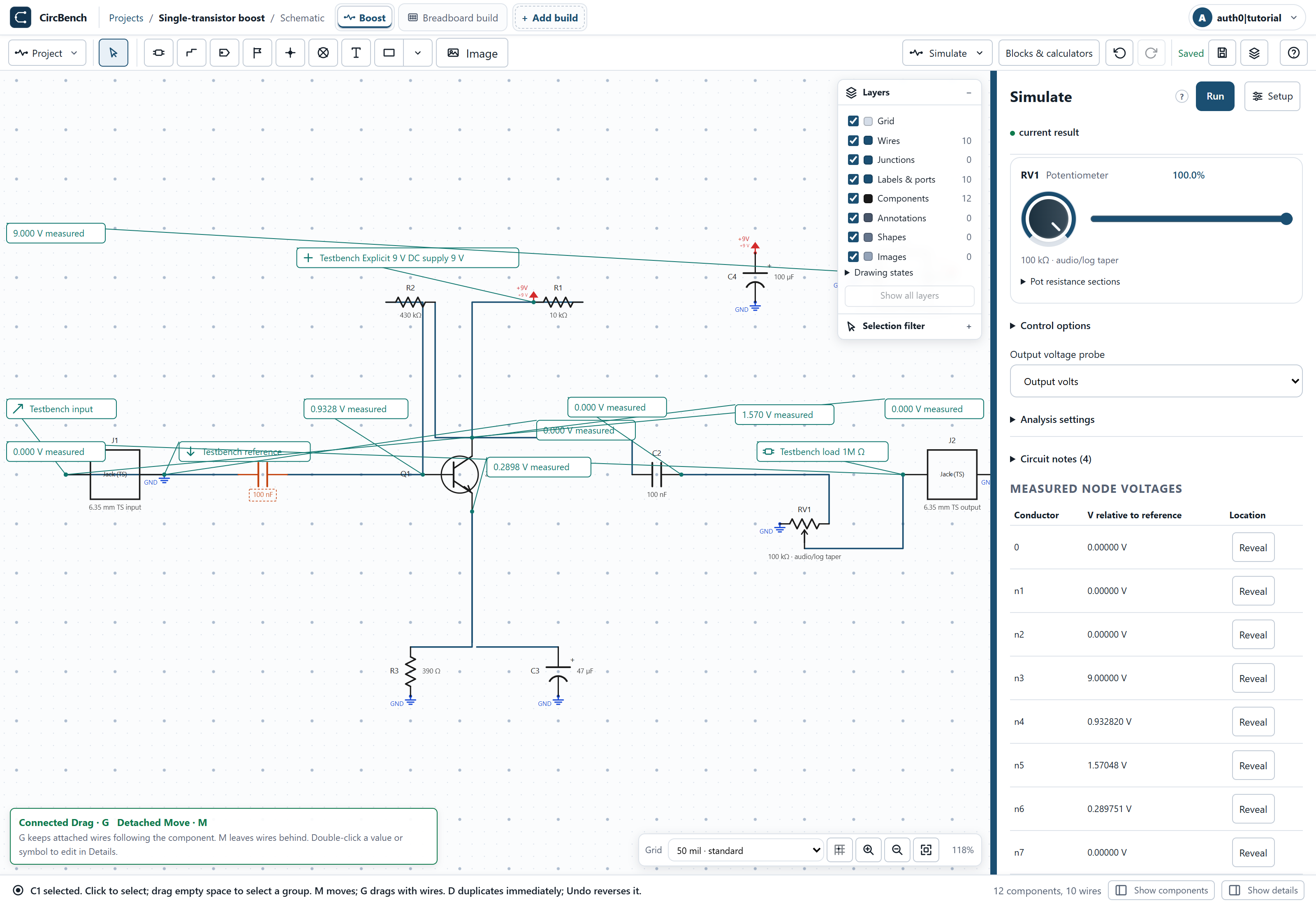
6. Inspect collector bias first
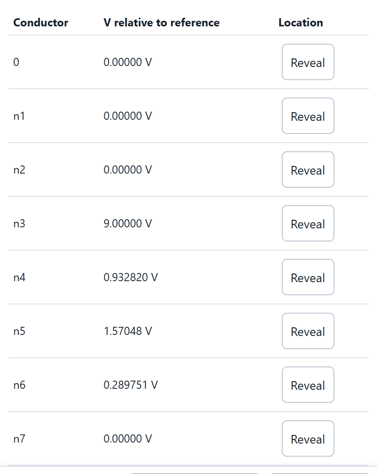
Run DC operating point. Wait for current result and use Reveal beside a node to locate it on the schematic. The reviewed nominal approximation places the collector around 1.57 V for this bench. Compare base, emitter and collector together: the available swing is asymmetric. An absent model, ground or return must be fixed before interpreting gain.
7. Read small-signal gain and phase
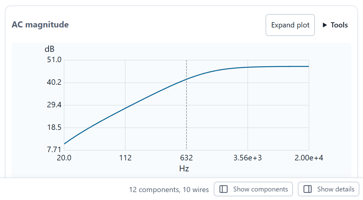
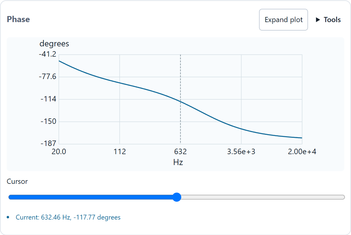
Run AC frequency response, 20 Hz–20 kHz. The two plots show gain in dB and phase in degrees around the DC operating point. Coupling and bypass capacitors make gain frequency-dependent. This linearized response describes small perturbations; it cannot supply the large-input clipping shape by itself. Keep the stated source and load while comparing curves.
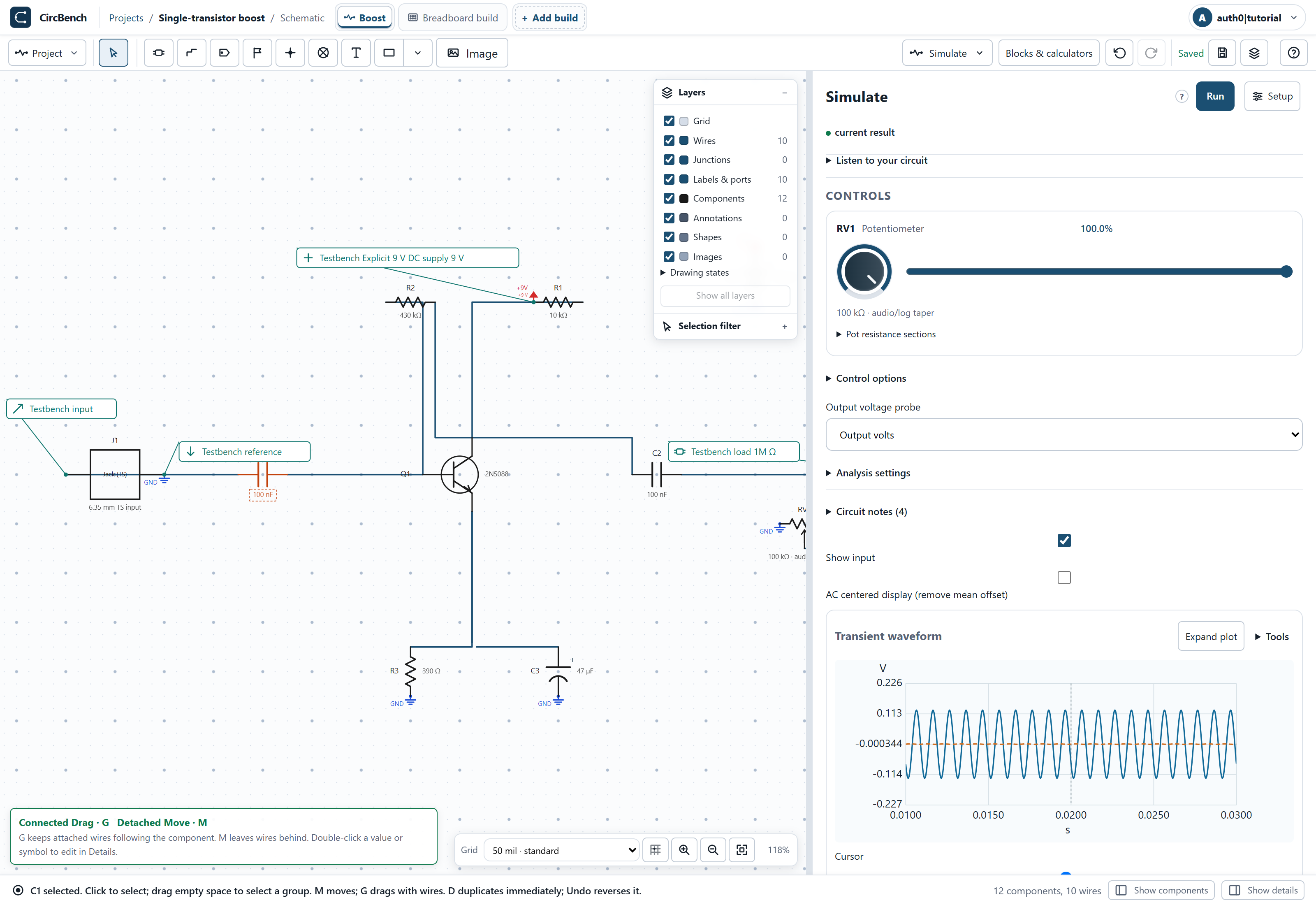
8. Run the small-input waveform
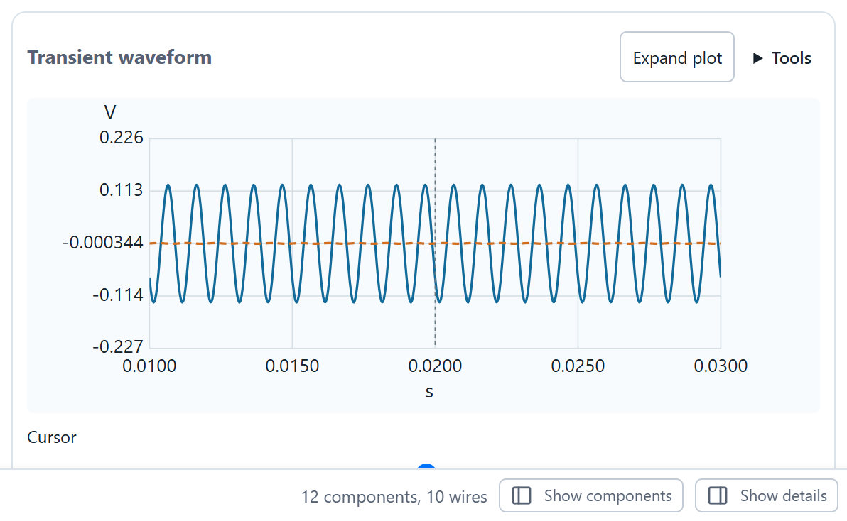
Run Transient waveform with the authored 1 mV-peak 1 kHz source. Compare dashed input with solid output, and note the inverted stage response. Use a settled portion of the plot. A cursor gives one sample; use several cycles to assess shape and amplitude. Keep level at 100% so comparisons use the same output division.
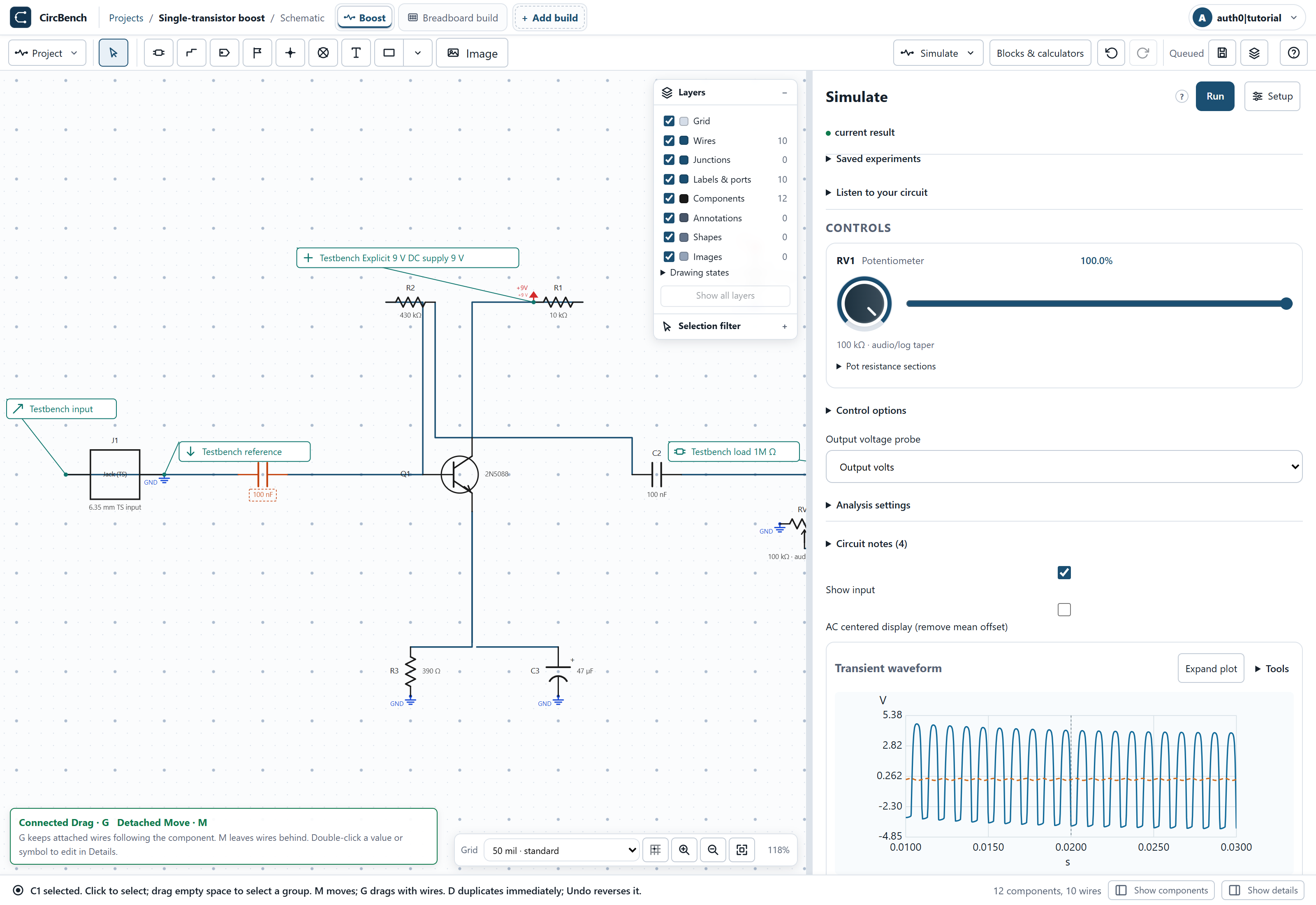
9. Deliberately overdrive the stage
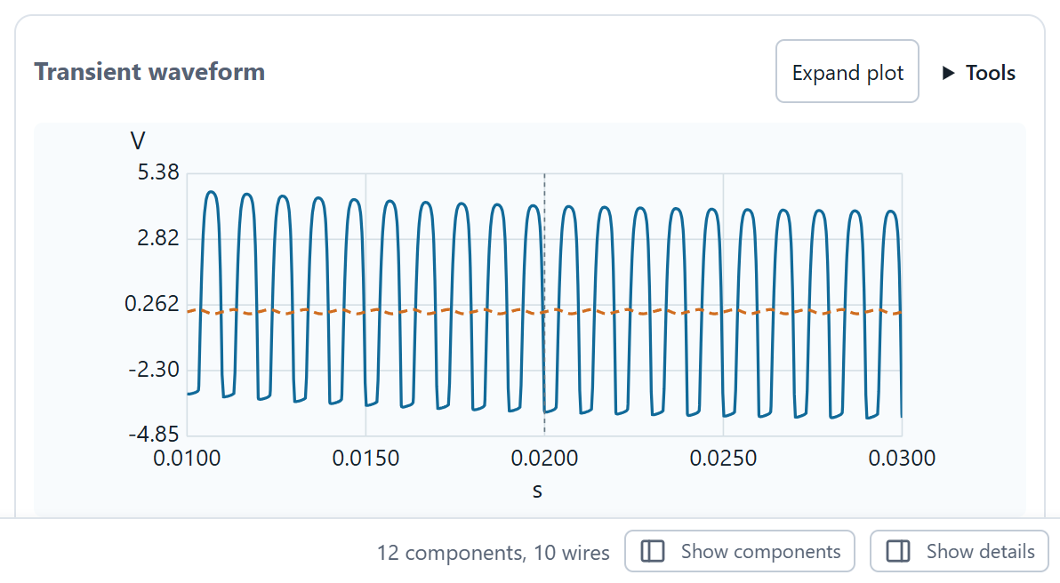
In Setup, change Transient peak amplitude to 0.1 V, save, and run a new waveform. Compare its flattening/asymmetry with the 0.001 V case. This is a source-amplitude experiment, not an increased supply or a resistor change. Restore 0.001 V and save before continuing; the last driven result is now previous until rerun.
Build the physical layout
10. Understand the breadboard groups
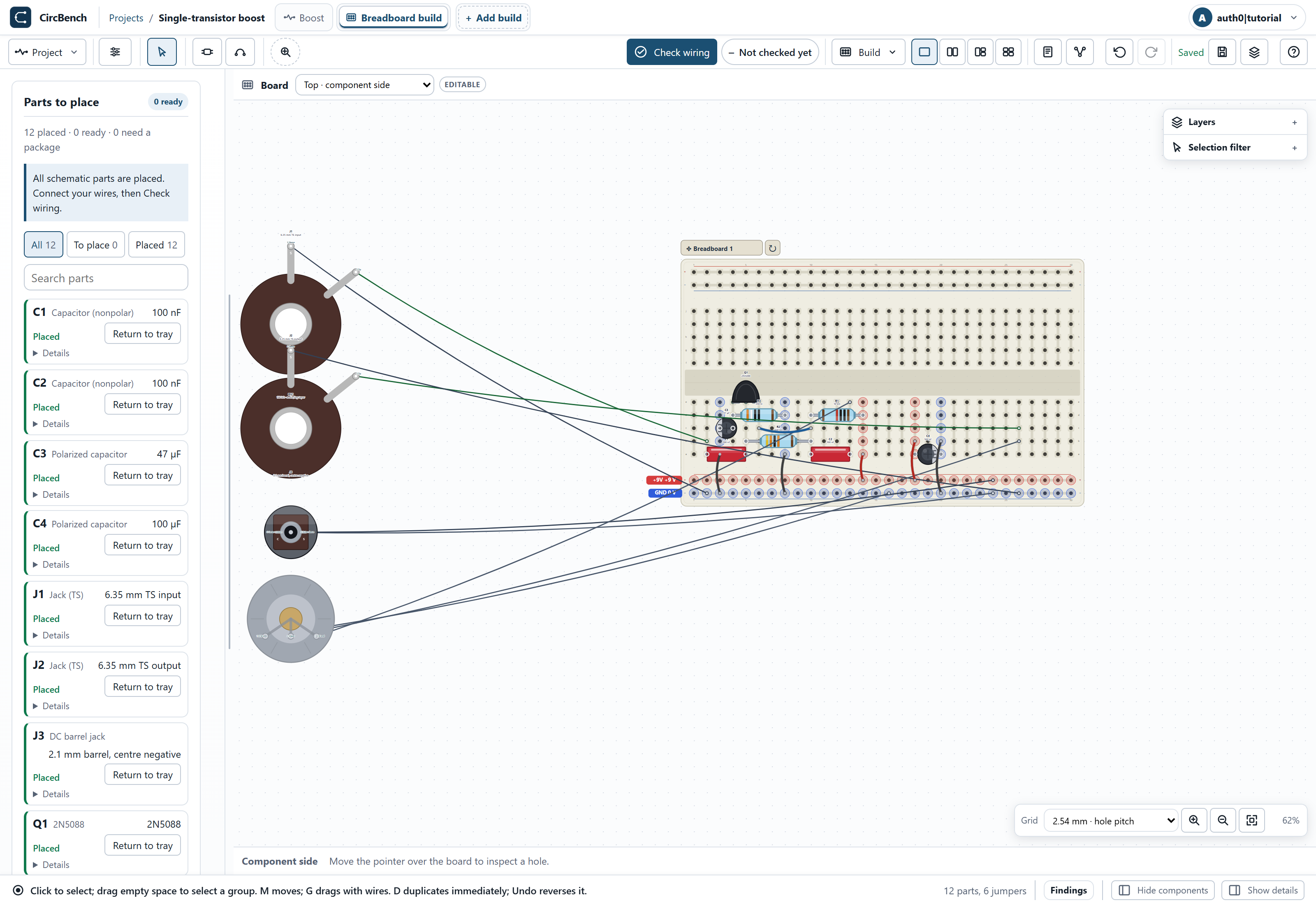
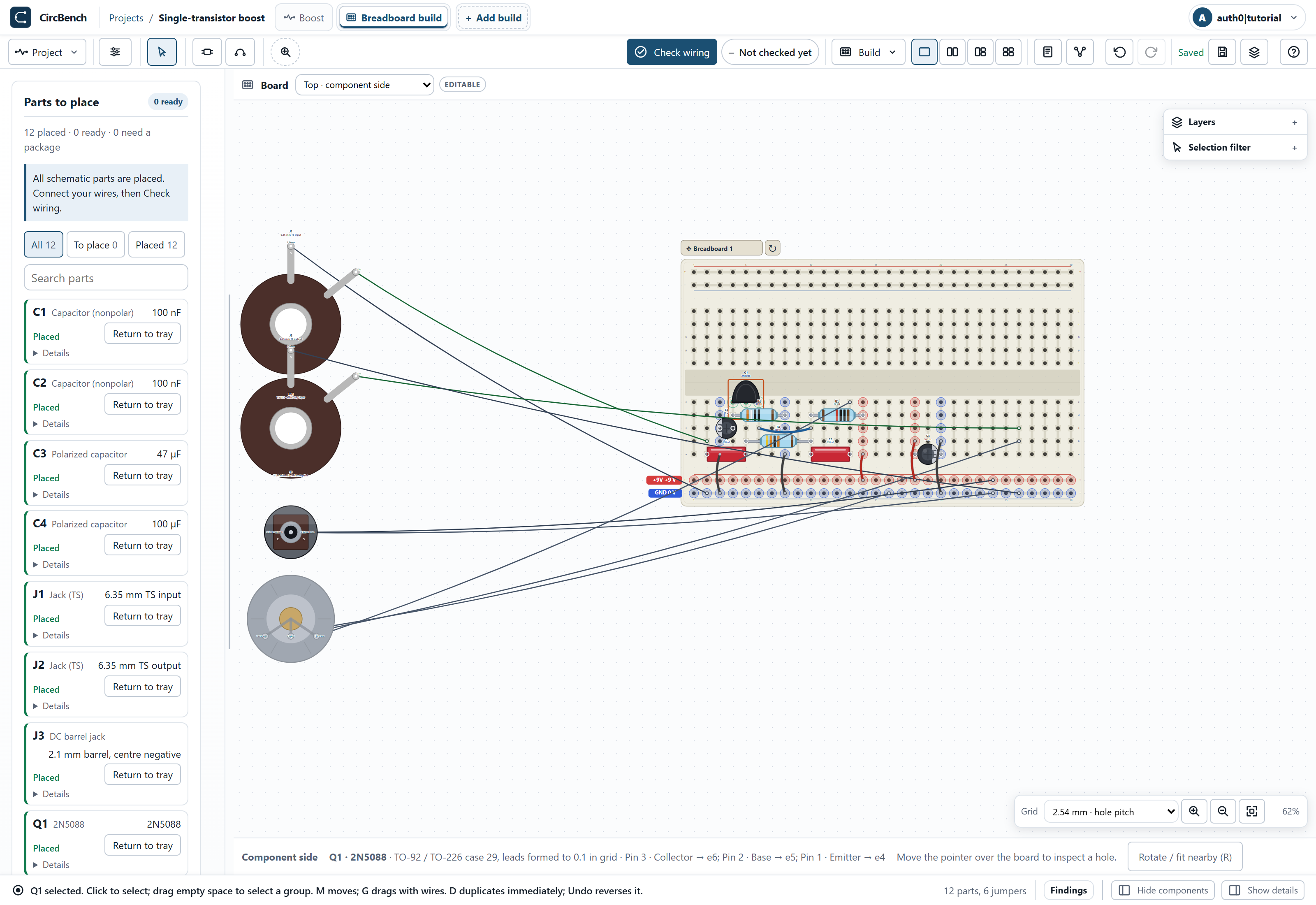
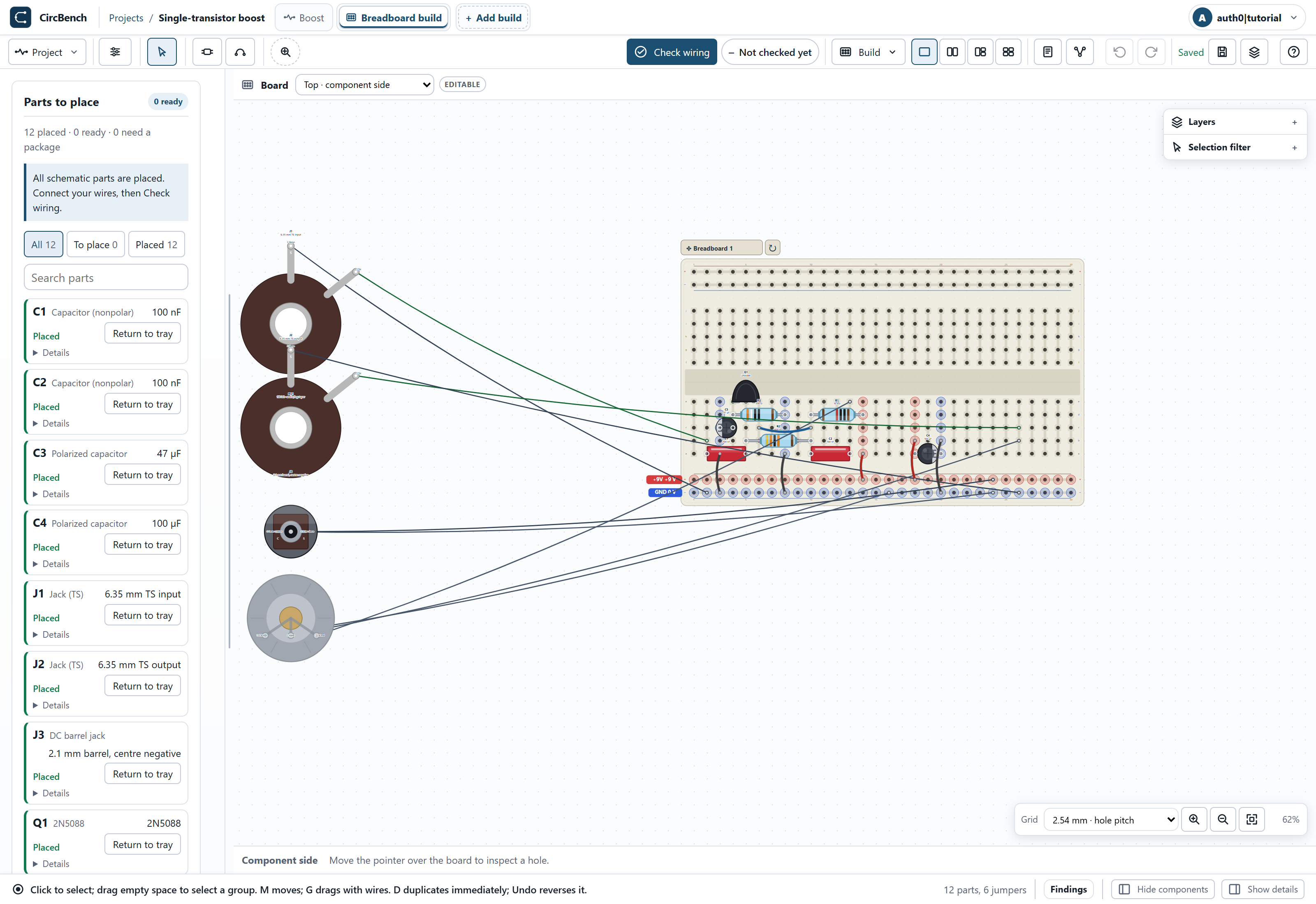
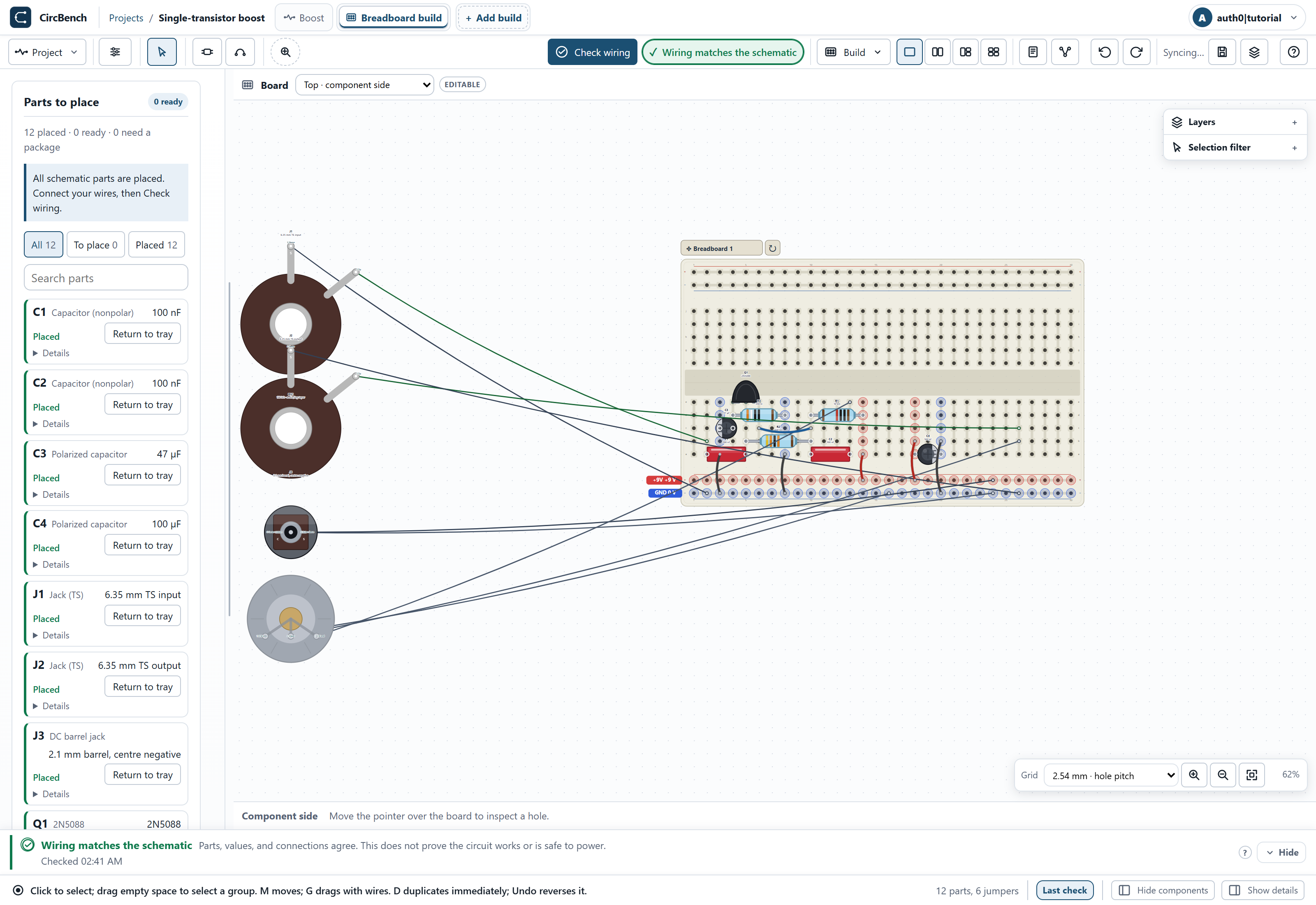
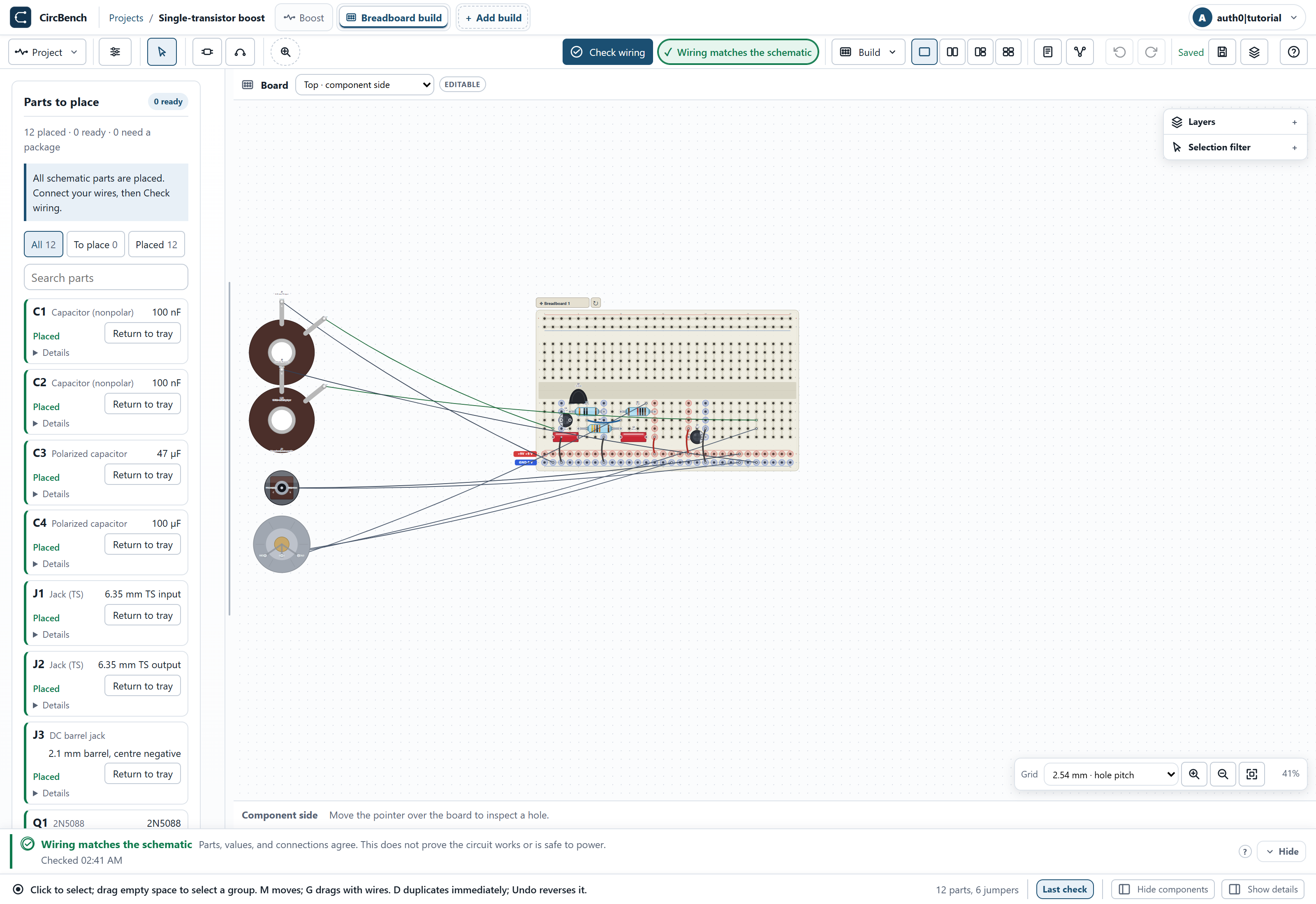
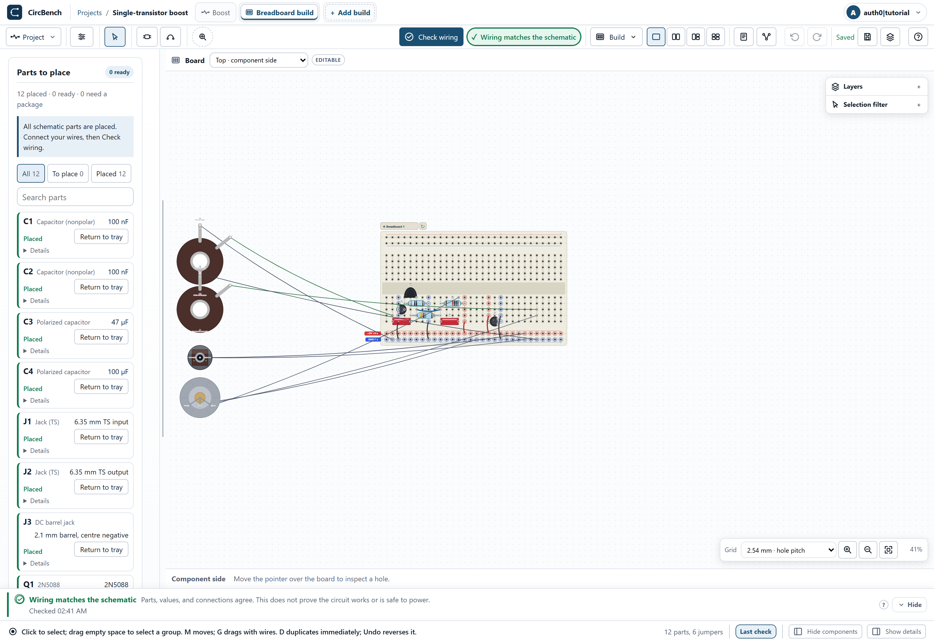
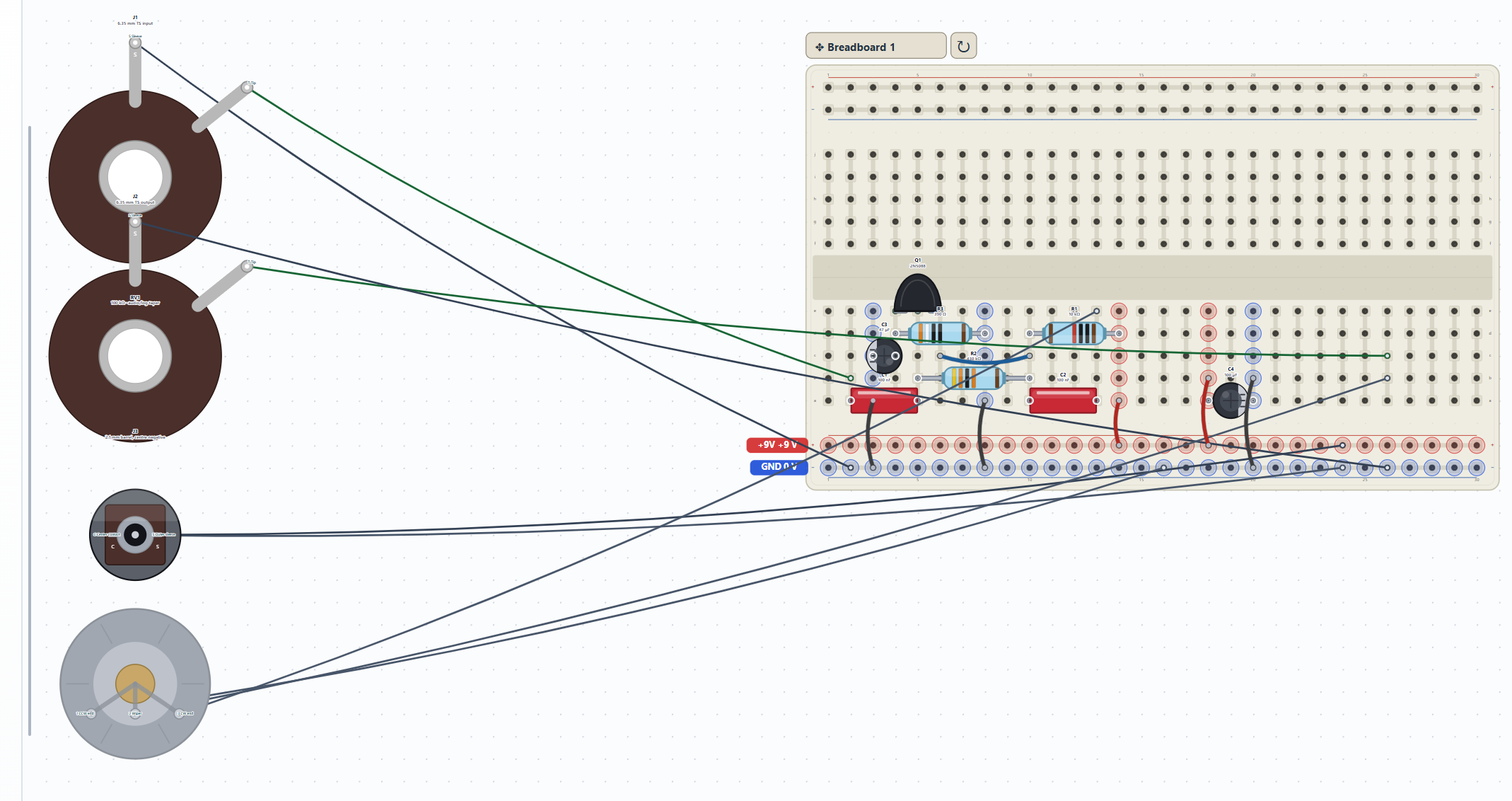
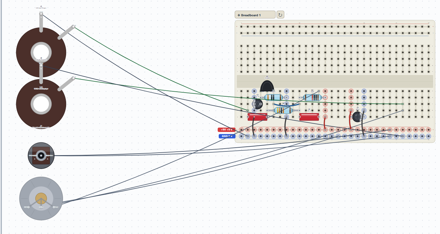
Open Breadboard build and Fit board to window. Use the half-size, 30-column template. Contacts a–e share each numbered terminal group; f–j form separate groups across the trench. Power rails are separate conductors. The picture shows the reviewed fit, not an instruction to assume every visible row or rail is joined.
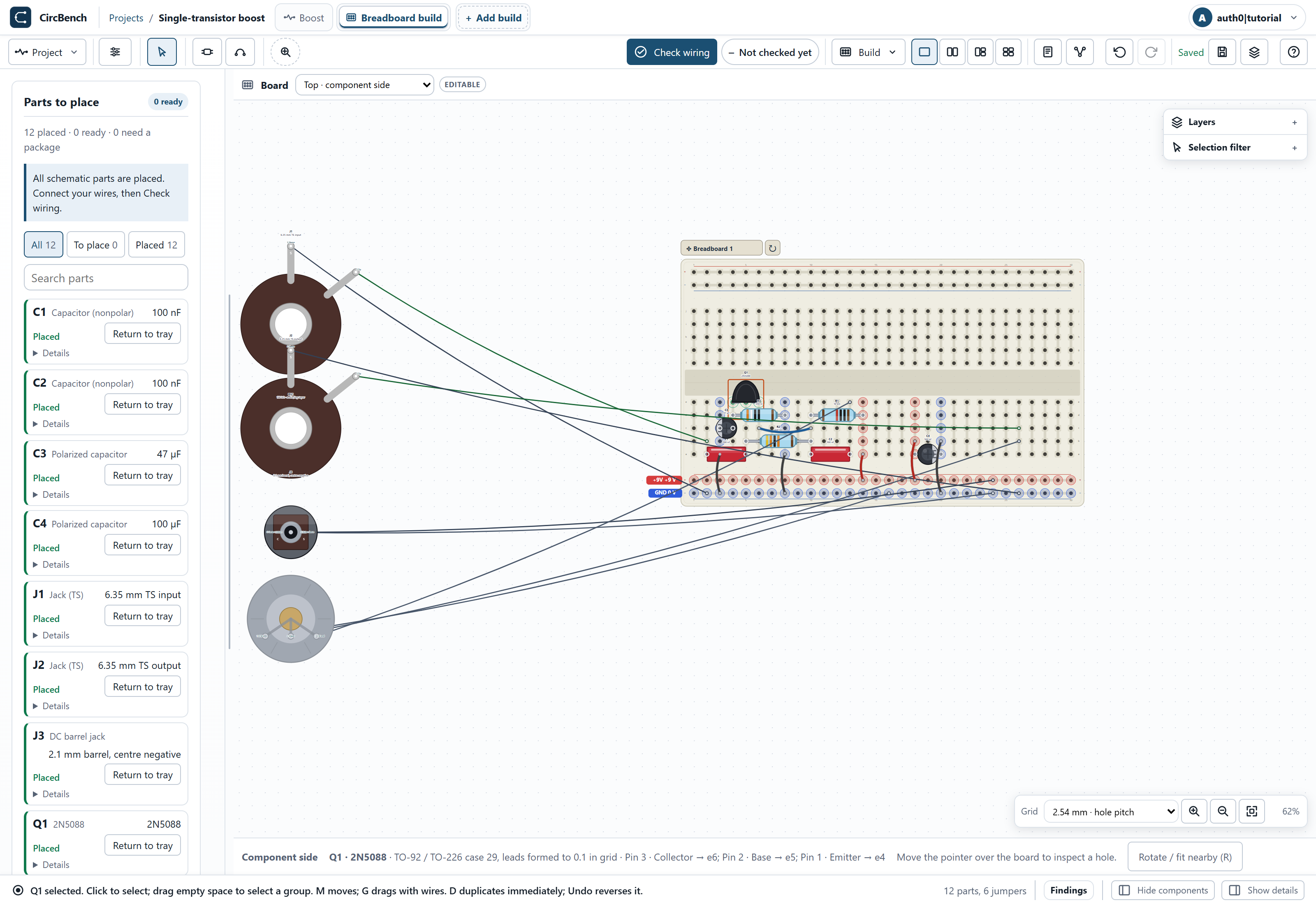
11. Check placement and polarity
Q1 E/B/C attach to e4/e5/e6. C1 spans a2/a5, R2 b5/b10, R1 d14/d10 and R3 d4/d8. C3 is positive c4, negative c3; C2 spans a10/a13; C4 is positive a18, negative a20. Inspect fitted pin-to-contact mapping before wiring; verify the actual purchased transistor’s pinout separately.
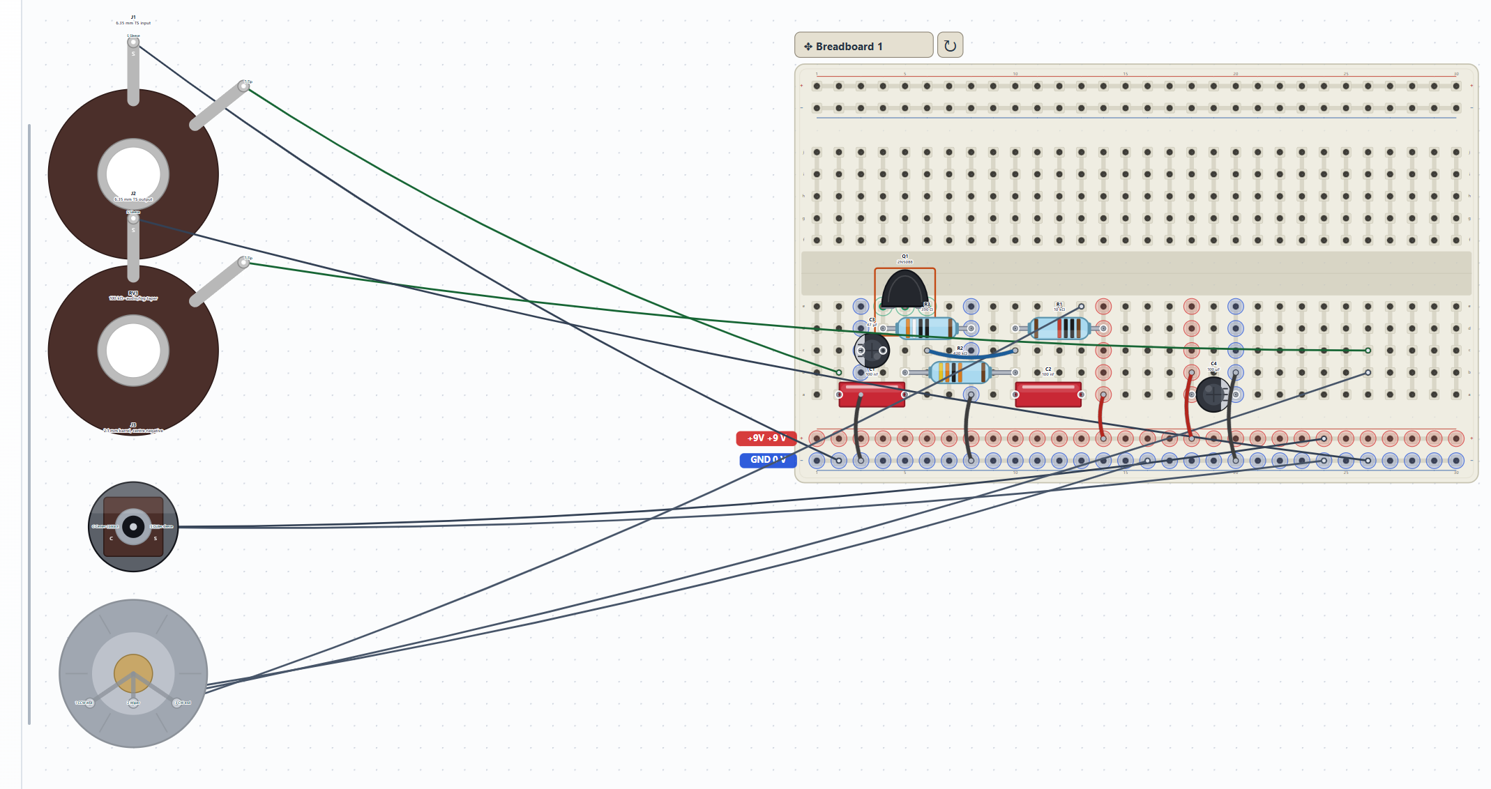
12. Add the six board jumpers
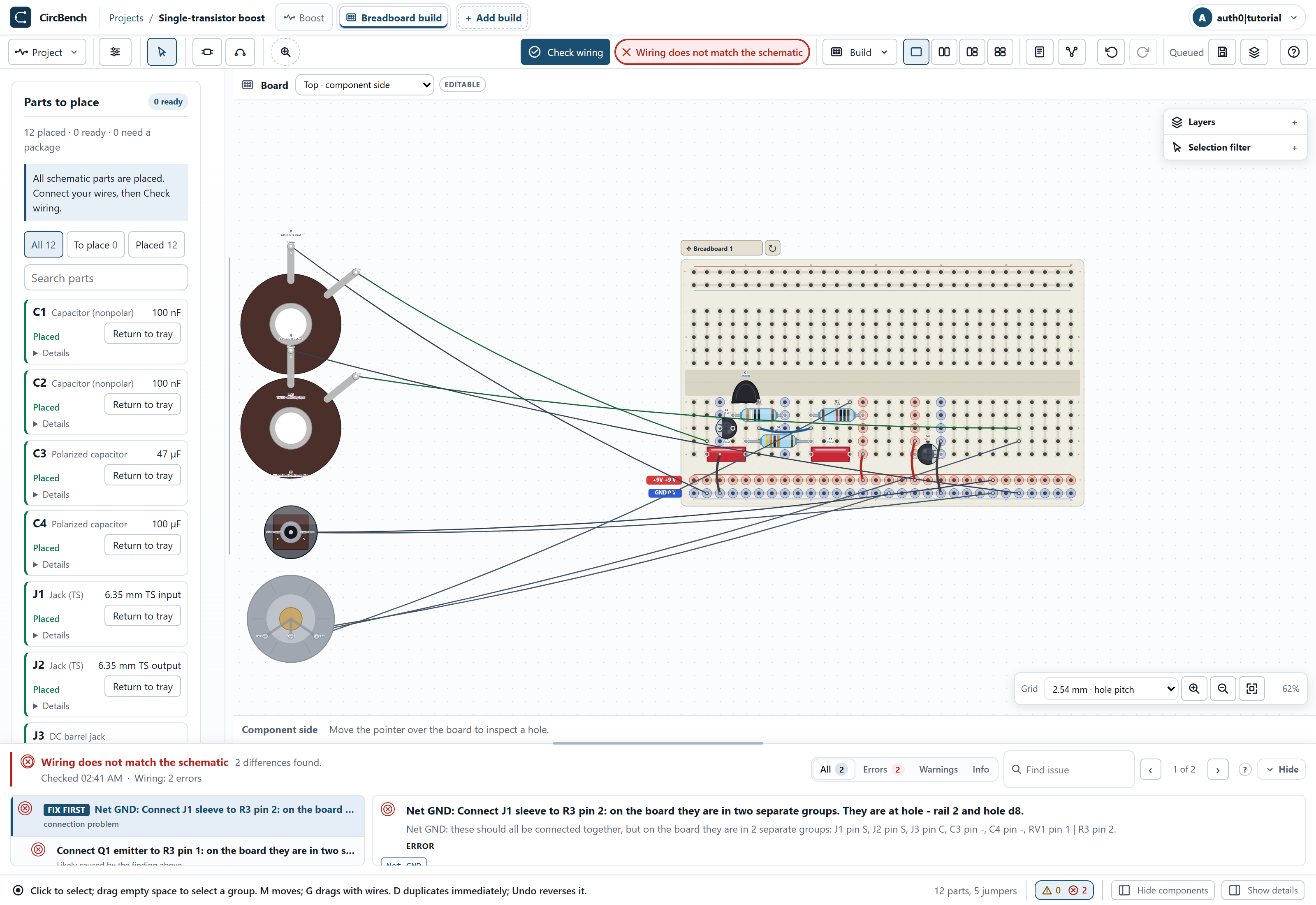
Reproduce c6–c10, a8–BN8, a3–BN3, a14–BP14, b18–BP18 and b20–BN20. These connect collector, emitter return, common return and supply groups that the breadboard does not otherwise join. Check the labels at both endpoints. Crossing the center trench visually, or drawing over a rail, does not create a connection.
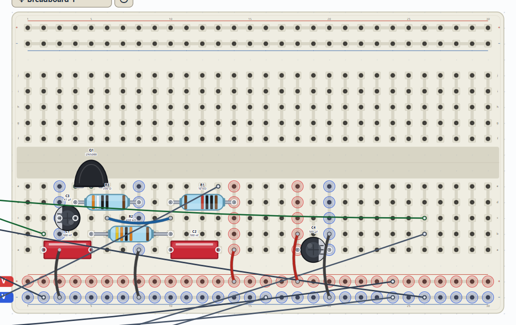
13. Complete the off-board harness
Follow the exact connection schedule below for the input/output jack, level pot and DC jack terminals. Keep sleeves and negative return together and the positive supply distinct. The example maps a center-negative supply connector; verify terminal identity in Details rather than inferring it from symbol position. This guide does not add an enclosure or bypass footswitch.
Exact reviewed connection schedule
The following tables come from the same versioned backup. Terminal identities belong to the fitted part; letter/number contacts belong to the board. In the copper view the picture mirrors, but these labels retain their identity.
| Part | Logical terminal → board contact |
|---|---|
| Q1 | E → e4; B → e5; C → e6 |
| C1 | 1 → a2; 2 → a5 |
| C2 | 1 → a10; 2 → a13 |
| R2 | 1 → b5; 2 → b10 |
| R1 | 1 → d14; 2 → d10 |
| R3 | 1 → d4; 2 → d8 |
| C3 | + → c4; - → c3 |
| C4 | + → a18; - → a20 |
| J1 | T → b2; S → BN2 |
| J2 | T → c26; S → BN26 |
| J3 | S → BP24; C → BN24 |
| RV1 | 1 → BN16; 3 → e13; W → b26 |
| Insulated connection | Endpoint A | Endpoint B |
|---|---|---|
| 1 | c6 | c10 |
| 2 | a8 | BN8 |
| 3 | a3 | BN3 |
| 4 | a14 | BP14 |
| 5 | b18 | BP18 |
| 6 | b20 | BN20 |
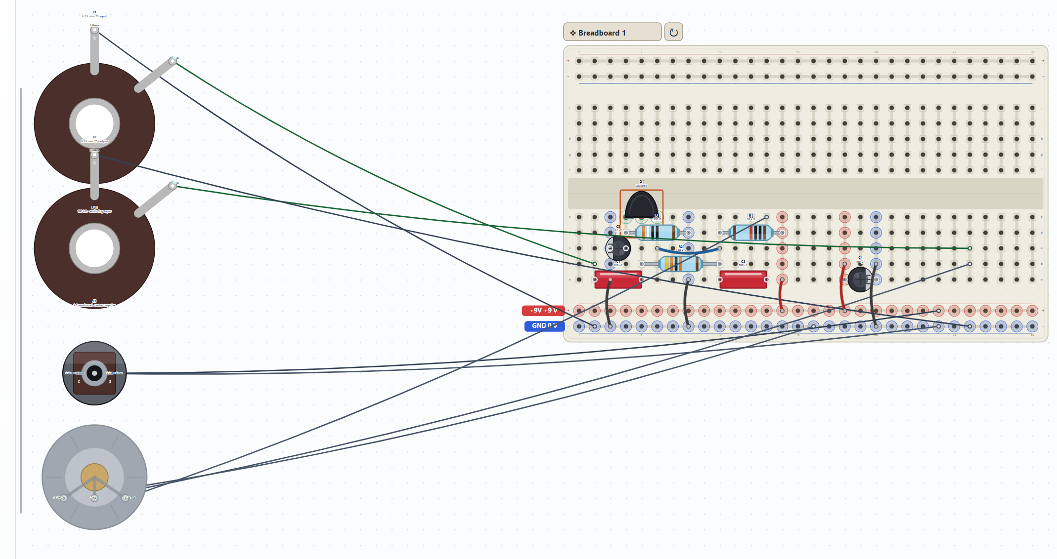
Check, repair and preserve the project
14. Run a fresh independent wiring check
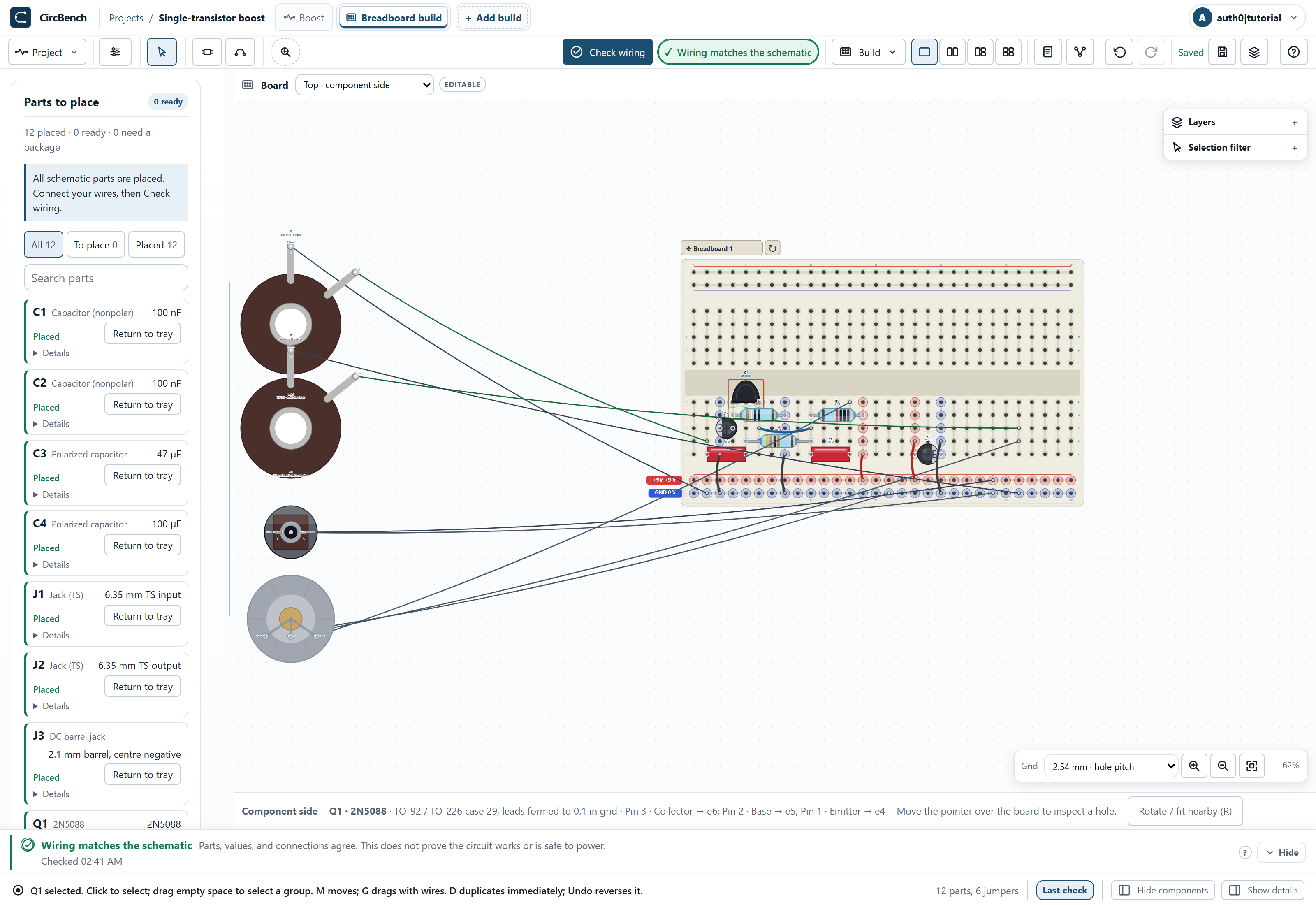
Choose Check wiring and wait for the completed match. CircBench extracts the represented board connections independently and compares them with the schematic. If your copy differs, reveal each reported open or short, verify both endpoints and check unplaced parts or fitted mappings. A previous or pending result is not a fresh match.

15. Introduce a deliberate wiring fault
Select the a8–BN8 emitter-return jumper and Delete it. Run a fresh Check wiring. The missing return produces an open in the physical build while the independent schematic simulation can still look plausible. Reveal the reported connection and compare the actual two endpoints; do not edit the schematic to conceal the broken jumper.

16. Undo the fault and prove the repair
Choose Undo to restore the deleted connection or cut. Run Check wiring again and wait for a fresh match. Undo alone is not verification: the completed check proves the represented topology was restored. Keep this repaired version for the following persistence and download checks.

17. Save, reload and check again
Wait for the normal save indicator, then reload the page. Open the same build and run Check wiring again. Confirm a fresh match after reload. If saving reports a problem, open save recovery and export a backup; do not assume remote account storage succeeded merely because the editor still displays the project.
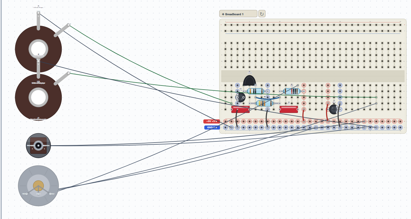
18. Inspect and export the parts list
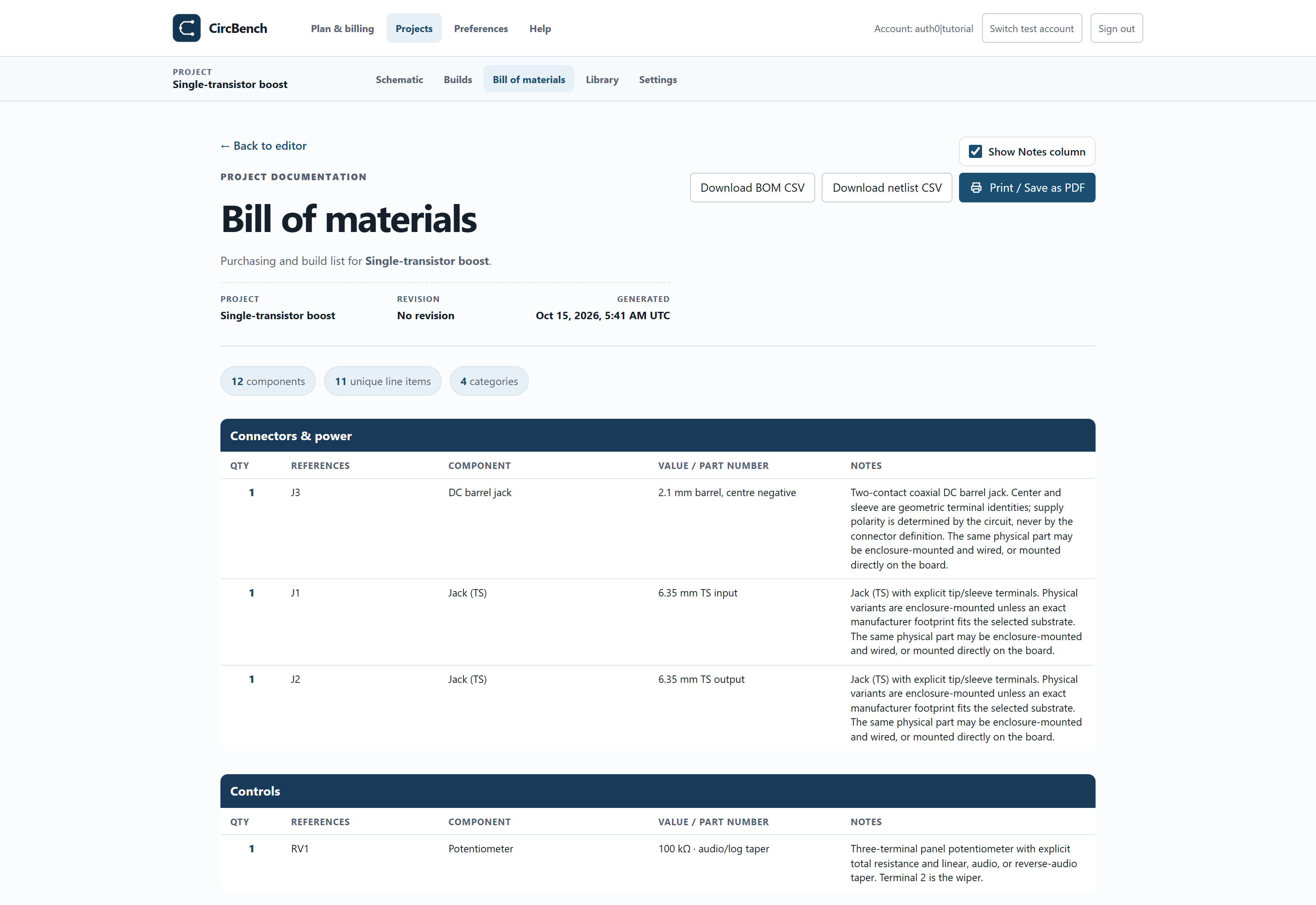
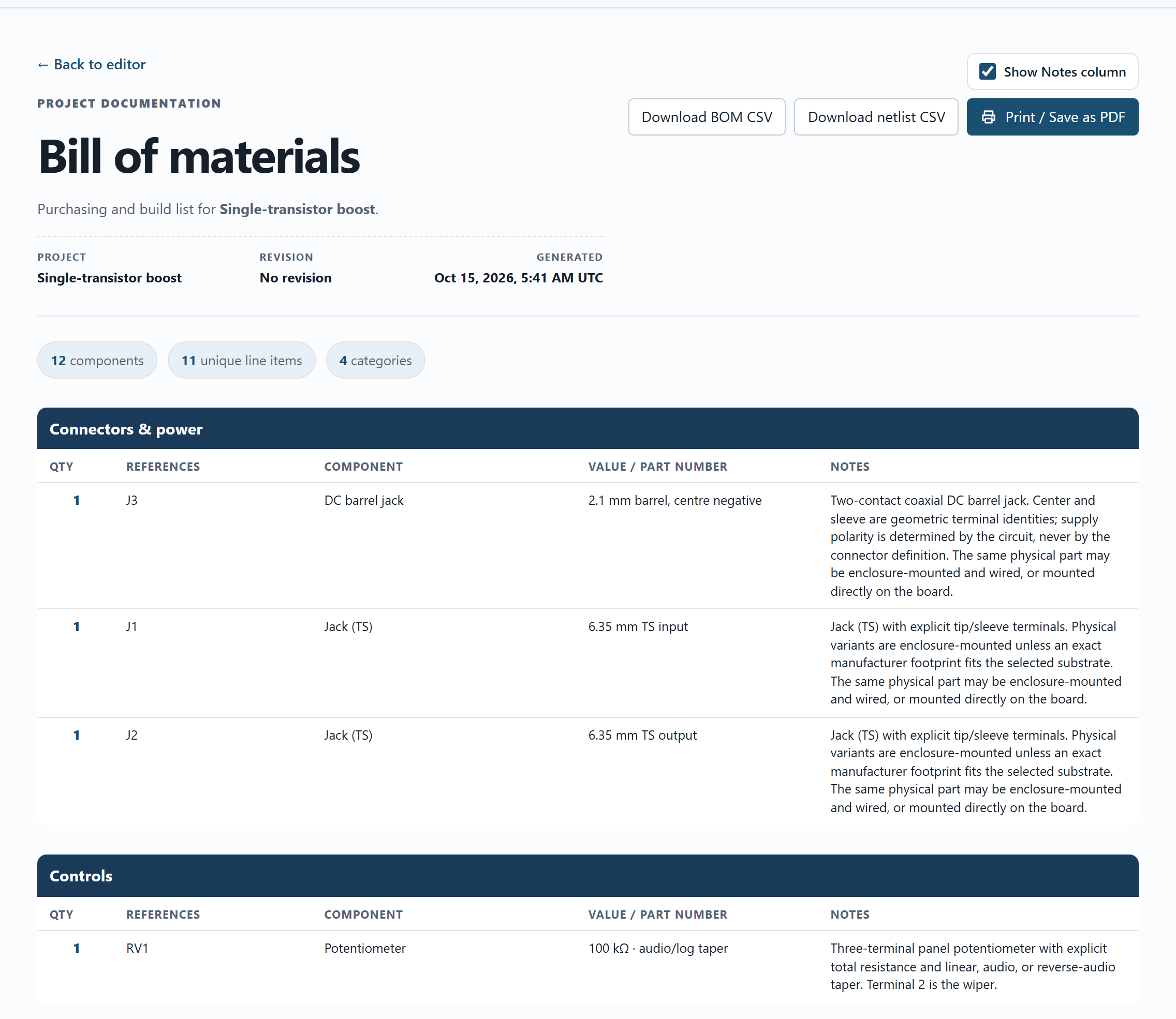
Open Bill of materials, review the fitted parts, values and quantities, then use Export CSV. Compare it with the versioned parts list above. A BOM lists represented parts; it does not select manufacturer voltage ratings or prove that a purchased package has the same terminal order. Resolve substitutions before physical assembly.
19. Export a portable project backup
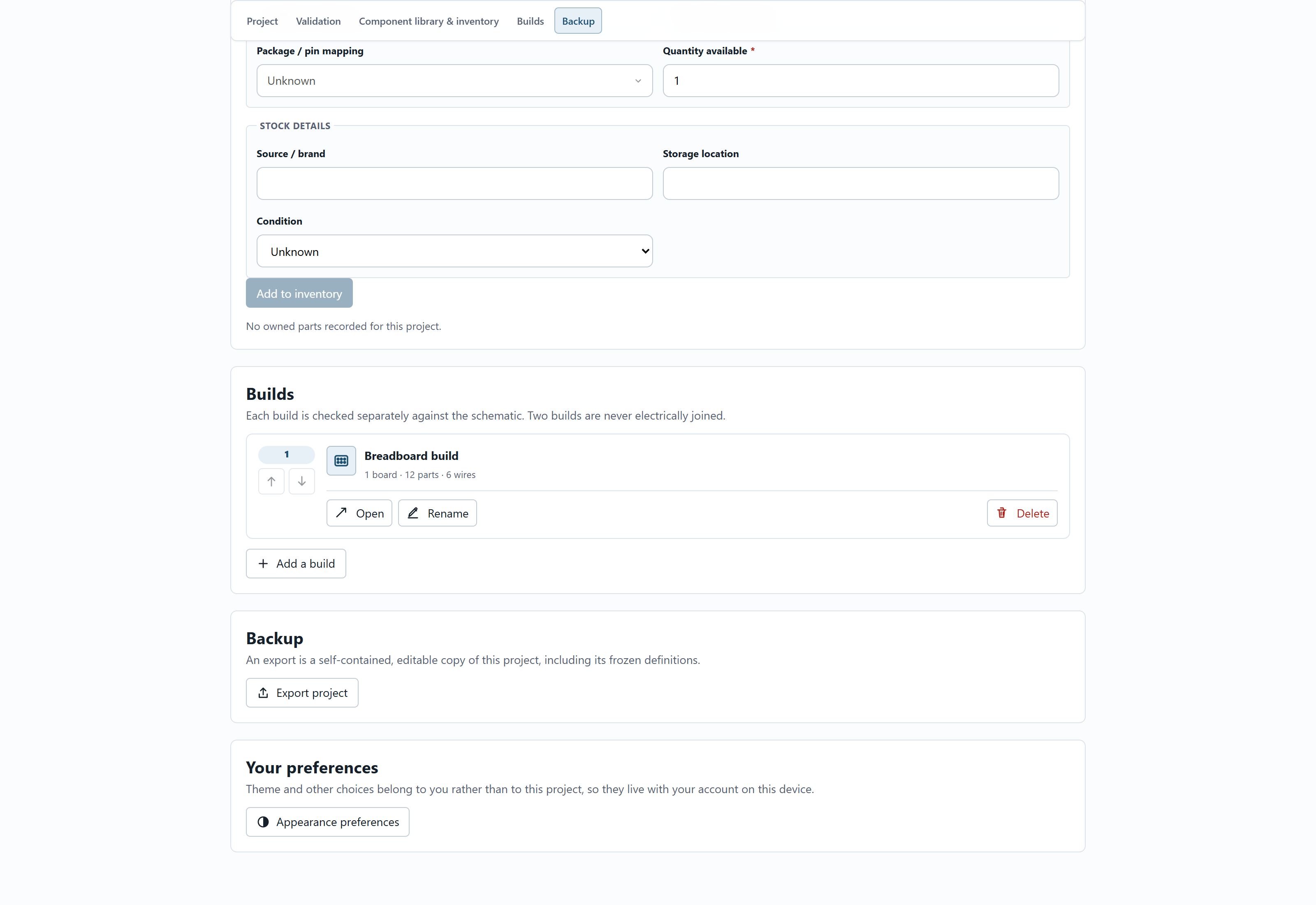
Open project Settings, go to backup and choose Export project. Keep the resulting .circbench.json file. This preserves the schematic, fitted build, definitions and saved bench/model settings. Raw simulation vectors and uploaded audio are separate outputs and are not retained in this project backup.

20. Import the backup and recheck
Return to Projects and Import the backup file. The imported copy appears in your library; explicitly Open its schematic, then its build. Run Check wiring and confirm a new match. If an import is rejected, keep the original file and compare its schema/version with the app rather than editing integrity fields by hand.
What this result establishes
The 2N5088 model is an authored nominal approximation. It does not qualify transistor spread, noise, thermal behavior, pickup interaction, maximum ratings or a physical pedal’s tone. Polarized capacitors and supply hardware still require real part and voltage-rating checks.
The screenshots show current solver results and fresh wiring checks for this exact example version. They do not assert that hardware was assembled, measured or qualified. Use the supplied source, load and stimulus settings when comparing results.
This is the CircBench-authored collector-feedback teaching boost and independently checked breadboard example. Its exact v2 project, embedded definitions and bench are preserved in the downloadable backup.
Your next project
Continue with the two-transistor stripboard fuzz to study coupled bias and deliberate distortion.